Opamp inverting amplifier.
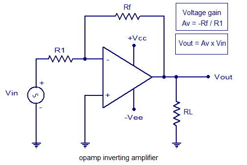
An inverting amplifier using opamp is a type of amplifier using opamp where the output waveform will be phase opposite to the input waveform. The input waveform will be amplifier by the factor Av (voltage gain of the amplifier) in magnitude and its phase will be inverted. In the inverting amplifier circuit the signal to be amplified is applied to the inverting input of the opamp through the input resistance R1. Rf is the feedback resistor. Rf and Rin together determines the gain of the amplifier. Inverting operational amplifier gain can be expressed using the equation Av = – Rf/R1. Negative sign implies that the output signal is negated. The circuit diagram of a basic inverting amplifier using opamp is shown below.

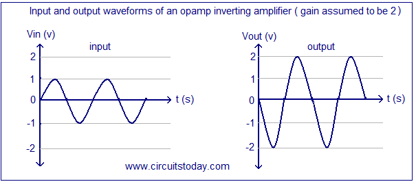
The input and output waveforms of an inverting amplifier using opamp is shown below. The graph is drawn assuming that the gain (Av) of the amplifier is 2 and the input signal is a sine wave. It is clear from the graph that the output is twice in magnitude when compared to the input (Vout = Av x Vin) and phase opposite to the input.

Practical inverting amplifier using 741.
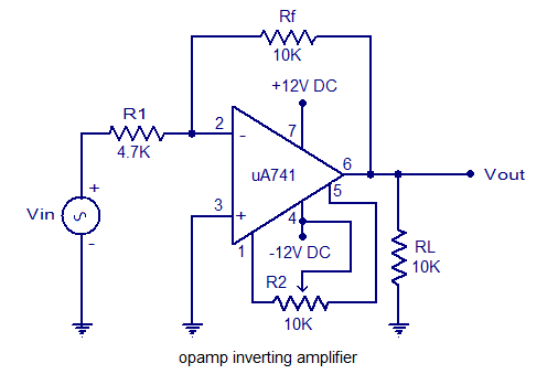
A simple practical inverting amplifier using 741 IC is shown below. uA 741 is a high performance and of course the most popular operational amplifier. It can be used in a verity of applications like integrator, differentiator, voltage follower, amplifier etc. uA 741 has a wide supply voltage range (+/-22V DC) and has a high open loop gain. The IC has an integrated compensation network for improving stability and has short circuit protection.

Signal to be amplified is applied to the inverting pi (pin2) of the IC. Non inverting pin (pin3) is connected to ground. R1 is the input resistor and Rf is the feedback resistor. Rf and R1 together sets the gain of the amplifier. With the used values of R1 and Rf the gain will be 10 (Av = -Rf/R1 = 10K/1K = 10). RL is the load resistor and the amplified signal will be available across it. POT R2 can be used for nullifying the output offset voltage. If you are planning to assemble the circuit, the power supply must be well regulated and filtered. Noise from the power supply can adversely affect the performance of the circuit. When assembling on PCB it is recommended to mount the IC on the board using an IC base.

9 Comments
but R1 is 4.7K so your sum doesn’t work?
thank u very much for your efforts
You even included My Favorite Op Amp Chip—The Great ua741,,,in a practical circuit!!!!
Nice Theory on The Operation of Op Amp, You even include a ACTUAL Circuit!!! Many Thanks!!!!