Differential amplifier
In this post, differential amplifier using BJT and differential amplifier using op-amps are explained in detail. Please go through both of them to get a better understanding.
The circuit diagrams and detailed equations are provided along with the article. Please go through them.
Differential Amplifier using Transistor
A differential amplifier is designed to give the difference between two input signals. The circuit is shown below.
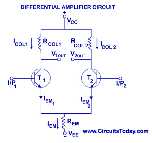
As shown in the circuit diagram above there are two inputs, I/P1 and I/P2 and two outputs V1OUT and V2OUT. I/P1 is applied to the base of the transistor TI and IP2 is applied to the base of the transistor T2. The emitters of both T1 and T2 are connected to a common emitter resistor so that the two output terminals V1OUT and V2OUT gets affected by the two input signals I/P1 and I/P2. VCC and VEE are the two supply voltages for the circuit. The circuit will also work fine using just a single voltage supply. You may have also noted that there is no ground terminal indicated in the circuit. Hence it must be automatically understood that the opposite points of both the positive and negative voltage supplies are understood to be connected to the ground.
Working of a Differential Amplifier
When a differential amplifier is driven at one of the inputs, the output appears at both the collector outputs. This is explained with a diagram below.

When input signal I/P1 is applied to the transistor T1, there will be a high voltage drop across the collector resistance RCOL1 , and thus the collector of T1 will be less positive. When I/P1 is negative T1 is turned OFF, and the voltage drop across RCOL1 becomes very low and thus the collector of T1 will be more positive. Thus we can conclude than an inserted output appears at T1’s collector for applying signal at I/P1.
When T1 is turned ON by the positive value of I/P1 , the current through the emitter resistance REM increases as the emitter current is almost equal to the collector current (IEIC). Thus the voltage drop across REM increases and makes the emitter of both transistors going in a positive direction. Making T2’s emitter positive is the same as making the base of T2 negative. In such a condition the transistor T2 will conduct less current which in turn will cause less voltage drop in RCOL2 and thus the collector of T2 will go in a positive direction for positive input signal. Thus we can conclude that the non-inverting output appears at the collector of transistor T2 for input at base of T1.
The amplification can be driven differentially by taking output between the collector of T1 and T2.
As shown in the figure above, if the transistor T1 and T2 are assumed to be identical in all characteristics, and if the voltages are equal (VBASE1 = VBASE2), then the emitter current can also be said to be eequal
IEM1 = IEM2
Total Emitter Current, IE = IEM1 + IEM2
VEM = VBASE – VBASE EM
IEM = (VBASE – VBASE EM)/REM
The emitter current IEM remains virtually constant regardless of the hfe value of the transistors.
Since ICOL1 IEM1, and ICOL2 IEM2, ICOL1 ICOL2
Also, VCOL1 = VCOL2 = VCC – ICOL RCOL, assuming collector resistance RCOL1 = RCOL2 = RCOL.
Differential amplifier is a closed loop amplifier circuit which amplifies the difference between two signals. Such a circuit is very useful in instrumentation systems. Differential amplifiers have high common mode rejection ratio (CMRR) and high input impedance. Differential amplifiers can be made using one opamp or two opamps. Both of these configurations are explained here.
Differential Amplifier using Op-amp
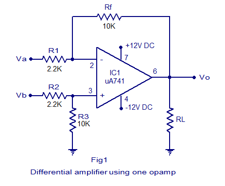
The circuit diagram of a differential amplifier using one opamp is shown below. R1 and R2 are the input resistors, Rf is the feedback resistor and RL is the load resistor.
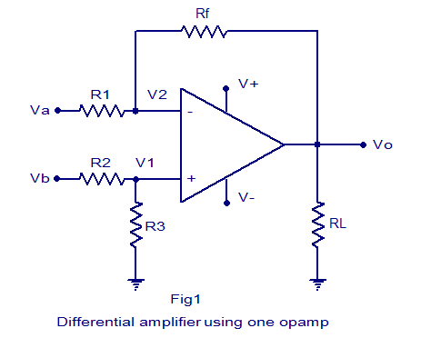
Derivation for voltage gain.
Equation for the voltage gain of the differential amplifier using one opamp can be derived as follows. The circuit is just a combination of an inverting and non inverting amplifier. Finding the output voltages s of these two configurations separately and then summing them will result in the overall output voltage.
If Vb is made zero, the circuit becomes an inverting amplifier. The output voltage Voa due to Va alone can be expressed using the following equation.
![]()
When Va is made zero the circuit becomes a non inverting amplifier. Let V1 be the voltage at the non inverting input pin. Relation between Vb and V1 can be expressed using the following equation.
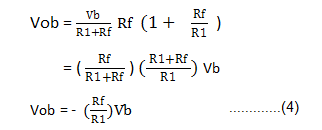
Output voltage Vob due to Vb alone is according to the equation
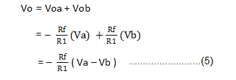
Then overall output voltage is
 Differential amplifier using two opamps.
Circuit diagram of a differential amplifier using two opamps is shown below. Main advantage of differential amplifier with two opamps is that it has increased overall gain. R1 is the input resistor for IC1 and R3 is the input resistor for IC2. Rf is the feedback resistor. Va and Vb are the two input voltages and they are applied to the non inverting inputs of IC2 and IC1 respectively. RL is the load resistor. V+ and V- are the positive and negative supply voltages.
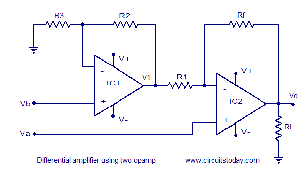
Derivation of voltage gain.
The equation for the output voltage V1 of the first opamp (IC1) is as follows.
 V1 and Va are the inputs for the second stage (IC2). Output voltage due to Va alone is.

Output voltage due to Vb alone is

Overall output voltage Vo = Voa + Vob
![]()
Let R1 = R2 and Rf =R1, then we have
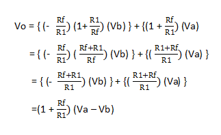
Therefore overall voltage gain Av can be expressed using the equation
![]()
Practical differential amplifier.
A practical differential amplifier using uA741 opamp is shown below. With used components the amplifier has a gain of around 5. Remember the equation Av = -Rf/R1. Here Rf = 10K and R1 =2.2K, -Rf/R1 = -10/2.2 = -4.54 = ~-5. Negative sign represents phase inversion. Use +/-12V DC dual supply for powering the circuit. uA 741 must be mounted on a holder.

9 Comments
Hi I would like to build voltage amplifier as weel as regulator using lm741. The input would be 0.05mv to 50volt. The input pulses per min would be 1-30000. The output pulse should be regulated 5 volt at all frequencies and voltage inputs. There would be only +12 volt source for powering the op-amp & not the -12v. The pin #4 will be grounded. Plz if anyone could help me.
I HAVE IMPLEMENTED DIFFERENTIAL AMPLIFIER USING TWO OP-AMP(324 WITH 12 VOLT D.C. SUPPLY).
VI1 IS KEPT AT 135 MILI-VOLT WRT V2.
I GET VOLT AT OUTPUT AROUND10.24 VOLT D.C.
ALL RESISTOR ARE AT 100 K.
THEORETICALLY O/P SHOULD BE 2X135 M.V=270 M.V.
PL. COMMENT
SANJAY AGARAWL
09968171133
in equation 4 for Vob how did you get the negative sign in the end?
it is used an inverting amplifier if input is positive output will be negative and vice versa.
CORRECTION OF OWN COMMENT:
In the derivation for the two opamp version, where you state
“Let R1 = R2 and Rf =R1, then we have”
I think it should be
“Let R1 = R2 and Rf =R3, then we have”
Thanks for the excellent text otherwise!
cheers!
Matjaz
HI!
I’m real hapy to your atticle,hopping I can use 741 in my project; currently I’m completting my circuit but the problem I face is how connect 4 sensor (weight sensor) before feeding them to circuit you described above (differential amplifier) and the output of 741 (opamp) will be inputed to my PIC16F84A
I took those sensors from a digital weight scale.because the output signal from the scale is very low that’s why I wanted to employ opamp to rise signal.
Having said those i hope you will help me to complte this task.
Please send information via my email (nziku99@yahoo.com)
the scale used 3v as power supply and my project eses 5v
PLEASE HELP!!!!!!
This shows real expertise. Thanks for the awensr.