The chip design includes different types of processing steps to finish the entire flow. For anyone, who just started his carrier as a VLSI engineer has to understand all the steps of the VLSI design flow to become good in his area of operations. There are different types of design procedures for analog/digital designs and FPGA designs. The analog design is mainly focusing on the back end design of a chip while FPGA on front end design.
Front End Design
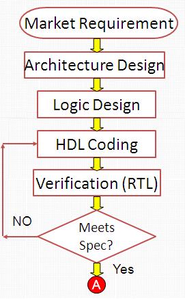
The steps involved are explained below.
Design entry: It describes the RTL (Register Transfer Level) logics in HDLs. For this, we use any of the hardware description languages (HDLs) such as verilog and VHDL. This design specification contains all the details which all are required for the design architecture, RTL block diagram, clock frequency, frequency domain details, waveforms, port details etc.
Logic Synthesis: The RTL logic written is synthesized to get the gate level netlist. This process can be done with the help of EDA tools. The code written can be implemented on an FPGA board only if, it is synthesizable.
Gate level simulation: The gate level simulation of the logic is very important in the verification. The functional check, timing checks and the Power analysis checks are included in the verification.
Back End Design
The back end design includes following steps.
Schematic entry: Using the cadence schematic editor in icms, you can create and extract the logic design you needed.
Pre layout simulation: The logic design is then verified, before doing its layout. The netlist of the schematic is generated and simulated using any of the tools such as Cadence ultrasim or Synopsys hspice. The working of each circuit can be checked using the simulation results.
Layout Design: After the schematic is simulated and verified, the corresponding mask layers of the circuit should be created which can be done using the Layout Editor by cadence. The layout design includes the floor planning, placement and routing. The locations of each schematic component are decided in the floor planning and are placed accordingly. While routing, the interconnections are done between the components.
Extracted simulation: The layout design should be extracted with the parasitics and simulate the system for performance using hspice or ultrasim. The parasitics can be either resistance or capacitances which are produced because of the interconnecting wires using for the routing. The parasitic components may affect the circuit performance badly. The parasitics cannot be avoided but can be reduced by proper routing. Finally the routed netlist that is called as GDS-II will be sent to the foundry and the chip will be manufactured as per the technology requirement.
Comments are closed.