Metal Semi-conductor FET (MESFET)
This article briefly describes the structure of MESFET , its comparison with MOSFET, D-MESFET and E-MESFET, circuit symbols, and also the characteristics of Schottky Barriers.
A post on MESFET has already been discussed. TAKE A LOOK : MESFET
This post also gives a brief description of MESFET and the main classification of MESFET.
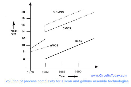
The gallium arsenide (GaAs) field-effect transistor (FET) is a bulk current-conduction majority-carrier device. This device is , is fabricated from bulk gallium arsenide with the help of high-resolution photolithography as well as ion implantation method into a semi-insulating GaAs substrate. The processing of this device is very simple as it does not need more than 6 to 8 masking stages. The figure below is used to compare the complexity in processing the device with the number of masks in the Y-axis and the function of time for both silicon and gallium arsenide technologies in the X-axis.

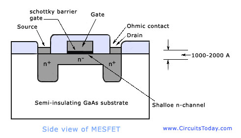
The structure of the basic MESFET as shown in the figure below is very simple. The MESFET has a thin n-type active region which is used to join the two ohmic contacts . A thin metal Schottky barrier gate is used to separate the highly doped drain and source terminals.

GaAs MESFETs are similar to silicon MOSFETs. The major difference is the presence of a Schottky diode at the gate region which separates two thin n-type active regions, that is, source and drain, connected by ohmic contacts. It should be noted that both D type and E type MESFETs, that is, ‘ON’ and ‘OFF’ devices, operate by the depletion of an existing doped channel. This can be compared with silicon MOS devices where the E [Enhancement] mode transistor functions by inverting the region below the gate to produce a channel, while the D [depletion] mode device operates by doping the region under the gate slightly in order shift the threshold to a normally ‘ON’ condition.
This similarity provides us with the basis for extending to gallium arsenic the design methodology used so successfully in silicon to simplify circuit as system design and layout issues.
The D-MESFET is normally ‘ON’ and its threshold voltage, Vtdep, is negative. The E-MES FET is normally ‘OFF’ and its threshold Vtenh is positive. The threshold voltage is determined by the channel thickness, a, and concentration density of the implanted impurity, ND. A highly doped, thick channel exhibits a larger negative threshold voltage. By reducing the channel thickness, and decreasing the concentration density a normally ‘ OFF’ enhancement mode MESFET with a positive threshold voltage can be fabricated. Circuit symbols for the depletion and enhancement mode MESFETs arc set out in the figure below.

The MESFET has a maximum gate to source voltage V of about 0.7-0.8 volt owing to the diode action of the Schottky diode gate. Since the principle underlying the operation of MESFETs is based upon the behaviour of metal-semiconductor interface, we will briefly outline some of the features that characterize such an interface.
Characteristics of Schottky Barriers
When a metal is brought into contact with a semiconductor, an electrostatic potential barrier (referred to as Schottky barrier) is created at the interface as the result of the difference in the work function of the two materials. To appreciate the physical nature of the barrier we can model the interface by visualizing a situation whereby the metal is gradually brought toward the semiconductor surface until the separation becomes zero.
As this separation between the metal-semiconductor surface is reduced, the induced charge in the semiconductor increases, while at the same time the space charge layer widens. A greater part of the contact potential difference begins to appear across the space charge layer within the semiconductor. Because the carrier concentration in the metal is several orders of magnitude larger than that in the semiconductor when the separation is brought to zero, the entire potential drop then appears within the semiconductor itself. This is in the form of a depletion layer situated adjacent to the metal and extending into the semiconductor.

4 Comments
sir how is that depletion layer forming in mesfet and what is the effect of that when we change the polarity of Vgs
Thanks for the useful article!
But MESFETs are still expensive compared to MOSFETs. A useful addition to this article (or a future one) would be WHEN to use them.
I still need more information on my school project concern about block diagram,circult &theory which is Design and construction of an Automatic car battery charge with a digital voltmeter display.
hello sir..
I am very grateful that i am getting all valuable article…
i need information regading Ig FET working and advantage in detail.. if possible mail me sir
thanks for ur great service to this e-world..
susindran, Research scholar