Nanotechnology – Tools and Instruments
In this article, the different tools and techniques that are used for producing and imaging a nanoscaled object is explained in detail. Atomic Force Microscope (AFM) and Scanning Tunneling Microscope (STM) is also explained in detail.
Before going into details, it is important that you know the basics of this article. Take a look at some of the links given below to know more.
Related Articles
- NANOTECHNOLOGY
- NANOMATERIALS
- MOLECULAR SELF-ASSEMBLY IN NANOTECHNOLOGY
- MOLECULAR NANOTECHNOLOGY (MNT)
- LATEST RESEARCH ON NANOTECHNOLOGY
- NANOELECTRONICS
In Nanotechnology, the main scanning probes that have been used from the beginning are the Atomic Force Microscope (AFM) and Scanning Tunneling Microscope (STM). Both the concepts are explained in detail.
Atomic Force Microscope (AFM)
Atomic force microscopy (AFM) is also known as Scanning force microscopy (SFM). This device is used to visualizing, imaging, taking measures and for manipulating objects that are in nanometre scale. The resolution of such a device is said to be in the order of fractions of a nanometre. The earlier version of the AFM was called the Scanning Tunneling Microscope, developed in the early 1980’s. The AFM was developed in the year 1986 by Binnig, Quate and Gerber at the IBM Research – Zurich and earned them the Nobel Prize for Physics for the same year.
The device consists of a mechanical probe that is used to sense the material that is placed on the surface. A highly accurate scanning procedure then takes place, through which the corresponding electronic signals are generated using piezoelectric materials. If the variations are deeper in scale, they can also be measured using conducting cantilevers.
Working of Atomic Force Microscopy (AFM)
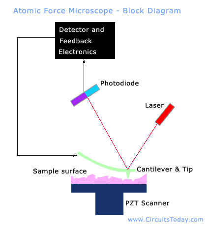
The block diagram of an AFM is shown below. From the figure it is understood that it has a sharp tip cantilever with a radius in nanometres, which is used to scan the surface of the material. The cantilever is made out of silicon or silicon nitride. The principle of Hook’s law is applied to the working of the cantilever. According to the law, a deflection will be produced by the cantilever as soon as the tip of it is brought closely to the surface of the material. This deflection is produced as a result of the forces that occur between the tip of the cantilever and the surface of the material.
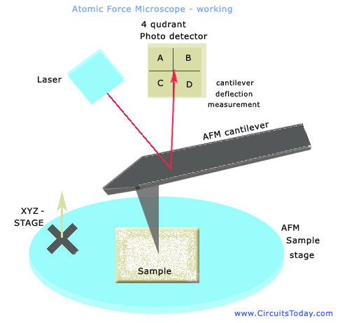
Many parameters can be measured with the help of an AFM. Some of the common measurements that are taken are chemical bonding, Van der Waals force, mechanical contact force, capillary forces, Casimir forces, and so on. If additional probes are fitted to the device, many other parameters can also be measured. The detailed working of an Atomic Force Microscope (AFM) is shown in the figure below.
The deflection produced by the cantilever will be measured using a series of photodiodes which receives the laser signal from the top tip of the cantilever. There will be a problem of the tip causing damage if it is scanned at a constant height. To overcome this problem, a feedback mechanism is used to keep the same force between the tip and the sample throughout. Thus the distance between the tip and the sample will remain constant always.
In the case of the sample, its force is kept constant by mounting it on a peizo-electric tube. This tube has the capability to move the material in the x, y and z-directions. The movement in the x and y directions help in scanning the sample. The movement in the z direction keeps the force constant.
More problems regarding the distortion due to a tube scanner can be eliminated by configuring three peizo-electric crystals.
Different Modes
Depending on the needs, the AFM can be operated in a number of modes. Some of the basic modes are explained below.
- Static or Contact Mode
In such a mode, the cantilever is moved across the surface of the material, which produces a deflection on the cantilever tip. This deflection is directly measured to know the value. In such an operation, the deflection on the tip is used as the signal for feedback. As the deflection can cause noise and drift to the signal, low stiffness cantilevers are normally used to amplify it. When the cantilever comes close to the material, the attractive forces tend to glue them. Thus this method is always done in a contact where a repulsive force is present.
- Dynamic or Non-contact mode
In this mode, the cantilever is made to oscillate externally with a frequency very close to its real value. The characteristics of the material will be attained from the comparison of the external reference oscillation with the changes in oscillation due to the forces developed between the tip and the material in close contact.
There is no contact between the tip of the cantilever and the surface of the material. The cantilever is made to oscillate at a frequency greater than its resonant frequency in which the oscillation amplitude may be below 10 nanometres.
The resonant frequency of the cantilever decreases due to the presence of van der Waals forces or any other forces that have the ability to move over the material surface. This decrease in the frequency is added to the feedback loop system to obtain a constant oscillation amplitude or frequency. This can be done only by moving the average cantilever tip to material surface distance accordingly. The material surface can be easily sketched by calculating the tip to sample distance at each data point.
This mode is more useful than contact mode as there will not be any kind of sample degradation effects. Thus this mode is used for measuring soft materials. But if a rigid material is to be measured, both the modes have the same characteristics. If the AFM works in contact mode, it is able to scan the liquid layer of the material to capture the underlying surface. But, in non-contact mode, the AFM oscillates above the adsorbed fluid layer so that both the liquid and the surface can be scanned.
- Dynamic Contact or Tapping Mode
Dynamic contact mode was designed so as to overcome the problem that a non-contact dynamic mode faces at ambient conditions. The materials tend to form a liquid meniscus layer at ambient conditions. As a result of this condition, the non-contact dynamic mode finds it difficult to adjust the distance between the cantilever tip and the surface of the material. As they tend to glue together, the dynamic contact mode was developed to overcome this problem.
Just like a non-contact mode, the tip of the cantilever is fixed to a peizo-electric material. This material oscillates the cantilever to an up and down movement to values near the resonant frequency. But, the amplitude of oscillation will be more than 10 nanometres and near to 100 nanometres. As the tip of the lever gets closer to the material, the amplitude of oscillation reduces due to the different interaction of forces on the cantilever. The distance between the lever and the material is controlled by an electronic servo. While the lever scans the material the electronic servo moves the height to the correct position.
Measurement of the deflection caused by AFM cantilever
As shown in the figure above, the solid state diodes reflects the light back to the cantilever which is absorbed by a position sensitive detector (PSD). The PSD has 2 diodes which produces two outputs. These outputs are given to a differential amplifier. As there is a slight angular displacement in the lever, one photodiode carries more light than the other one. Thus, the output of the differential amplifier will be proportional to the deflection of the cantilever.
Other Tools and Techniques
- The very first devices that made us possible to see the nanoparticles were the scanning confocal microscope and the scanning acoustic microscope in the years 1961 and 1970. The latest techniques involve a method called position assembly in which the end of a scanning probe is used to make the nanoparticles visible.
- Some of the other tools that are needed in this field are for the application in nanolithography, a process that is used to reduce a big material to nanosize. Some of the methods that are used for this technique are optical lithography, X-ray lithography, dip pen nanolithography and so on.
- Different tools and techniques are also required for the fabrication of nanowires like electron beam lithography, nano-imprint lithography, atomic layer deposition, molecular vapour deposition, and so on. Techniques required for molecular self assembly also require tools.
Scanning Tunneling Microscope (STM)
Scanning Tunneling Microscope (STM) was developed in the year 1981 by Gerd Binnig and Heinrich Rohrer. An STM is used for imaging surfaces at the atomic level. The lateral resolution of an STM lies around 0.1 nanometre and depth resolution lies around 0.01 nanometre. This measure is more than enough to manipulate a good image. With this resolution, individual atoms within materials are routinely imaged and manipulated.
This method can be used in different modes like air, water, high vacuum, liquid and gas. It can also be used in very high and low temperatures. In an STM, when the tip of the device is brought near the material, a difference in voltage is applied between them. This difference causes the electrons to move through the empty space created between them. Such a method is called quantum tunneling.
As a result, a current is formed which depends on the position of the tip of the device, the applied voltage, and the local density of states (LDOS) of the sample. The image is displayed on a monitor according to the scanning process of the tip on the material.
The method is very precise unless and until the parameters are maintained according to standards. The tip of the device should be sharp, the surface should be clean and stable, the device should have better control on the vibrations produced.
Components used in STM
- Scanning tip
- Piezo-electric controlled height
- X-Y scanner
- Coarse sample-to-tip control
- Vibration isolation system
- Computer
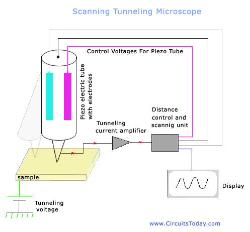
Working of Scanning Tunneling Microscope
The tip of the device is moved closer to the sample in a controlled manner. At the same time a voltage difference is brought to the tip of the device. As soon as the tip reaches very close to the material, the voltage difference is turns off. The working of the device is clearly shown in the figure below. Take a look.

When the tip reaches close to the material, piezo-electric effect causes the accurate control of the tip. At such a situation the distance between the tip and the material is usually between (4-7) Å. At the same time the voltage difference in the tip causes the electrons to flow between the sample and the tip. This causes a current flow, whose reading is noted. As soon as the tunnelling effect starts to work, the distance between the tip and the material can be changed accordingly. An image is created according to the current readings. A movement of the tip in the X-Y direction causes a change in the height and density of the states. The height is in the Z-axis and can be measured with respect to a constant current. This method is called constant current method. In another method called the constant height method, the change in current with respect to position can be measured itself.
The image clarity depends on the radius of curvature of the scanning tip of the device. The image can also be distorted if the tip of the device has two ends rather than one. If such a condition occurs, it will lead to tunnelling effect from both the tips. Such a condition is called double-tip imaging. The material used for making the tip is mostly tungsten or gold. The tip is designed using electro-chemical etching.
The body of the STM has to be highly rigid in order to avoid the sudden isolations that may occur during the scanning process. If such a problem happens the current to height ratio changes thus deforming the image.
The computer is responsible for keeping the position of the tip in the correct position w.r.t the sample, sample scanning and also data acquisition.


1 Comment
It is very nice note which I learnt….