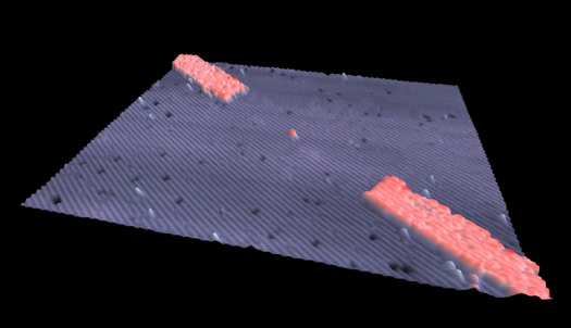
A group of researchers including Michelle Simmons and her colleagues developed a single phosphorus atom transistor using a Scanning Tunneling Microscope (STM) at the University of New South Wales. The 3-dimensional perspective of the device is shown in the figure above. Till date, this is known to be the smallest transistor ever built, and ever to be built in future. Thus, this device will be known to be the stepping stone to quantum computers.
The single phosphorus atom device was manipulated using the STM. Using the STM to design and control nano-scale circuits was very difficult. But, the researchers used a number of STM combinations along with unique etching skills to make a transistor with a precise location on a silicon surface. Though many other single atom transistors have been developed before, this is the first time that the researchers were able to apply a small voltage in a controllable manner. As shown in the image, the single atom is placed in the center and the red shaded regions form the electrical leads.
A silicon atom out of a six atom group is interchanged with one phosphorus atom. The atom is placed between source and drain terminals. The distance between them is less than 20 nanometers. The gate electrodes are almost 100 nanometers apart. The changes in the electron states were studied after applying a small voltage between the sets of electrodes. The output produced clearly showed the characteristics of a Field Effect Transistor (FET). That is, the output current produced depends on the voltage applied.
This device has proved to be controlled with nanowires and can be packed very close to each other to build powerful microprocessors. But, the only disadvantage is that the transistor characteristics were successful only in highly cold temperatures. That is, temperatures of that of liquid helium (-391 degree Fahrenheit). The researchers are trying to rectify this problem.


13 Comments
THE NUCLEI OF THE ATOMS MUST BE MADE STATIONARY WITH RESPECT TO THE ELECTRON FLOW AND “HAND OFF LOCI” TO WORK. ANY FORM OF ENERGY TRANSDUCTION WILL UPSET THAT BALANCE BY ALTERING THE ENEGERY LEVEL, AND THE ATOMIC SUB- PARTICLE COOPERATION REQUIRED FOR SOUGHT QUALITY OF BEHAVIOR.TRANSDUCTION OF ANY WAVELENGTH HAS ISSUES ASSOCIATED WITH THE SUBSTRUCTURE OF THE ATOM WHICH IT RESONATES. I SUGGEST A MAGNETIC ‘BUBBLE’ WHICH CAN CREATE A SEPARATE “DOMAIN” THAT INTERACTS WITH EARTH MAGNETIC DOMAIN AS ITS OWN ENTITY LOCKING THE ATOMS IN A PATTERN THAT WILL DETER AND CONTROL ANY ENERGY TRANSDUCTION AND OTHER INTERRUPTING ELEMENTS EFFECTIVE WITHIN THE DOMAIN OF THE TRANSISTOR STRUCTURES AND SUPPORTING ELEMENTS OR WORKING CONSTRUCTS.
Wow !
Fantastic work guys !
I hope IBM or INTEL would support these brilliant folks out there and sponsor their projects and experiments .
I suggest they should email Microsoft about that so the company would help them develop the concept into real usable durable and public micro computer systems .
On the other hand we , here in egypt , are facing an internet speed of 128 kilobytes per second or a 512 KB/s as a maximum !
Amazing and wonderful, let’s wait for its come out from experimental lab and real practical uses. Thanks for sharing.