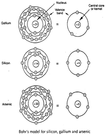
In this post, the origin of Gallium and Arsenic, as well as the structure and properties of the Gallium Arsenide (GaAs) crystal is explained in detail. The atomic structure of Gallium and Arsenic are explained with diagrams and also compared with Silicon. The valence configuration of Ga, As and Si is also shown.
Before going into details, it is better to know the basics on GaAs in VLSI technology. Click on the link below.
TAKE A LOOK : ULTRA-FAST SYSTEMS AND GaAs VLSI TECHNOLOGY
Gallium (Ga), a toxic material, is produced as a by-product in both the zinc and aluminium production processes. Similarly, arsenic (As), which is also very toxic, is produced from ores such as AS2S3 or AS2S4. The oxidation reaction of the ores is first entailed to produce AS2O3. Later through the reduction with carbon, arsenic is produced.
In order to better appreciate the structure and the properties of gallium arsenide crystal, it is better to know more about the characteristics of the individual atoms, Arsenic and Gallium. The figure below shows Bohr’s model of the atomic structures for gallium and arsenic. For the sake of better understanding, they are also compared with Silicon.
Gallium has a positively charged nucleus of +31, while the arsenic atom’s nucleus has a positive charge of+33. In both the cases, the total positive charge of the nucleus is equalized by the total effective negative charge of the electrons.
Electrons, travelling within their respective orbits, possess energy since they are a definite mass in motion (that is, rest mass of electron is 9.108*10-23gm). This means each electron in its relationship with its parent nucleus exhibits an energy value and functions at its own energy level. This energy level is dictated by the electron’s momentum and its physical proximity to the nucleus. The closer the electron is to the nucleus, the greater is the holding influence of the nucleus on the electron and the greater is the energy required for the electron to break loose and become free.
Due to the ability of the outer orbit electrons to break loose from the parent atom, they are known to be stronger than the inner orbit electrons. That is why, the outer orbit electrons are also referred to as ‘valence electrons’. The outer orbit in which valence electrons exist is called the ‘valence band’. It is the electrons from this band that are being considered in much of the discussions in the section to follow.
Crystal chemical bonds result through sharing of valence electrons. In materials such as Si, Ga and As, the outer-shell valence configuration is shown below.
Si→3s2 3p2
Ga→4s24p1
As→4s2 4p3
Here the core is not shown and the superscripts denote the number of electrons in the subshells (that is, s and p orbitals).
To know about the semiconductor structure and doping process of GaAs click on the links below.
TAKE A LOOK : GALLIUM ARSENIDE (GaAs) DOPING PROCESS


1 Comment
“Gallium (Ga), a toxic material,”
Gallium isn’t toxic!!! The main reason for any toxicity is due to arsenic, not the gallium!!!