If the load resistance RL is reduced or load terminals are shorted accidentally, a very large load current will flow. It may destroy the pass transistor Q1, diode or possibly some other component. Fuse protection will not prove adequate because the transistor may get damaged in a very small fraction of a second
To avoid this situation, a current limiting circuit is added to a series regulator, as illustrated in the figure.
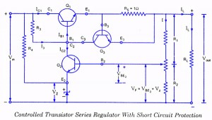
The current limiting circuit consists of a transistor Q3 and a resistor R5 (approximately 1 ohm) connected between base and emitter terminals of transistor Q3. With normal load current, transistor Q3 remains off because the voltage drop across resistor R5 is small (less than about 0.7 V necessary for making the transistor Q3 on). Under this condition, the circuit works normally, as described above. With the excessive load current (exceeding 0.6/1, that is, 0.6 A or 600 mA) the voltage drop across R5 becomes large enough to turn transistor Q3 on. The collector current of transistor Q3 flows through R3 thereby decreasing the base voltage of transistor Q1. This results in reduction of the conduction level of transistor Q1. Thus further increase in load current is prevented.
Figure summarizes the current limiting. When load resistance RL is infinite, the output voltage is regulated and has a value of VREQ. The load current IL is zero for this operating condition. When RL decreases, the load current IL increases upto the point where RL becomes equal to RL(min) At this minimum load resistance, IL equals 600mA and VBE equals 0.6V. Beyond this point, transistor Q3 turns on and the current limiting sets in. Further decrease in RL produces decrease input voltage, and regulation is lost. When RL is zero, the load current IL is limited to a value between 600 m A and 700 m A. The load current with shorted-load terminals is symbolized as ISL. When the load terminals are shorted in fig. 30.9, the voltage across resistor R5 is
VBE = ISL R5 or ISL = VBE / R5
where VBE is typically between 0.6 and 0.7 V.
The minimum load resistance where regulation is lost can be estimated with the following equation
RL(MIN) = VREG / ISL
The exact value of RL (min) will be slightly less or greater than this.
The simple current limiting circuit also has a drawback of large power dissipation across the series pass transistor. With a short across the load, almost all the input voltage appears across the pass transistor. So the pass transistor has to dissipate approximately
Pv = (vin-vBE)ISL.
where VBE is the base-emitter voltage of Q3, the current-limiting transistor.
Foldback Current Limiting
A problem with the simple current limiting circuit just discussed is that there is a large amount of power dissipation in series pass transistor Q1 while the regulator remains short-circuited. The foldback current limiting circuit is the solution of above problem.
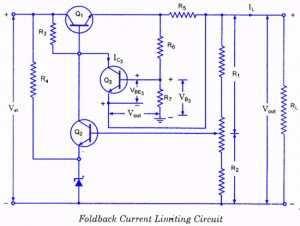
The circuit of a transistor series voltage regulator with foldback current limiting facility is illustrated in the figure. In this circuit base of transistor Q3 is biased by a voltage divider network consisting of resistors R6 and R7. The load current IL flows through resistor R5, causing a voltage drop of IlR5(approximately) across it. Thus a voltage of (IlR5 + Vout) acts across the voltage divider (R6 – R7) network. The voltage applied to the base of transistor Q3 is equal to the voltage drop across resistor R7 and is given as
VB3 = (R7 / R6 + R7) (IL R5 + Vout)
Emitter of transistor Q3 is connected to the positive terminal of Vout. Applying Kirchhoff’s voltage law to closed mesh of Q3 shown in the figure we have
Vout + VBE3 = VB3
or VBE3 = VBa – Vout = K (ILR5 + Vout) – Vout = K IL R5 + (K – 1) Vout where K = R7 / R6 + R7
Thus the magnitude of base drive of transistor Q1 is by this Vbe3. Now if load resistance decreases, may be due to any reason, load current IL will increase causing voltage drop Il,R5 to increase. This causes VB3 to increase and therefore Vbe3 to increase. This makes transistor Q3 on in a stronger way. The increased collector current Ic3 of transistor Q3 flows through the resistor R3 thereby decreasing the base voltage of transistor Q1 This results in reduction of the conduction level of transistor Q1. Thus further increase in load current is prevented.
From the equations above it is obvious that VBE in this circuit is much more than that was in circuit illustrated in the above figure(only ILR5). It means that the increment in load current is limited by larger amount in circuit shown in figure.
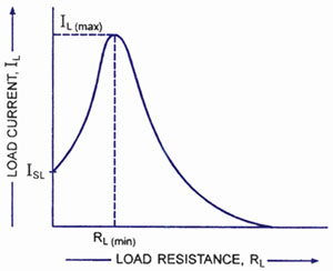
Due to reduction in load resistance RL, VBE3 increases to a level so that transistor Q3 gets saturated. Now collector current Ic3 becomes constant. Any further decrease in RL will have no effect on Ic3 . The corresponding load current is ILmax) and is given as
ILmax = VBE3/KR5 + (1-K) * Vout
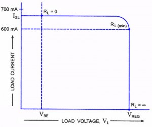
Beyond this point VBE3 also drops due to saturation. Therefore according to equations given above load current IL begins decreasing with decrease in RL from RL(min), as illustrated in figure given above. When load resistance RL is zero that is, when output terminals get shorted the output voltage Vout becomes equal to zero. Substituting Vout = 0 in the above equation we have
ISL = VBE3/KR5
That is, shorted-load current ISL is very much smaller than maximum load current ILmax) proving the foldback current limiting. The smaller ISL limits power dissipation
in pass transistor Q1 preventing it from being damaged. This is the main advantage of this circuit.
Transistor Current Regulator
Transistor current regulator using a Zener diode and a PNP transistor is shown in the figure below. The main function of this regulator is to maintain a fixed current through the load despite changes in terminal voltage.
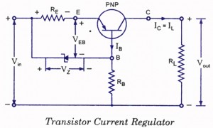
Suppose due to increase in output voltage Vout load current IL increases. This causes an increase in collector current Ic, because Ic = IL.
The increase in Ic causes an increase in IE (because IE = Ic) resulting in decrease in VEB due to increased voltage drop across RE. With decrease in VEB, conduction level reduces and collector current decreases. Thus load current is maintained constant.
A similar logic applies in case of decrease in load current IL.

5 Comments
The current limiting circuit consists of a transistor Q3 and a resistor R5 (approximately 1 ohm) connected between base and emitter terminals of transistor Q3* It should be Q1. Hope other theory are fine.
Hi it is correct, the corrent sensing is between base and emitter of Q3 whose collector is connected to Q1 base to remove its bias once the current exceeds the set limit.
Kazkokia nesvankybe…
Thanks for such an informative article. but i’ve pointed out something that you should look ……. in fold back protection circuit discription, don’t you think that formula for maximum load current (Imax) is wrong? i think the term (1-K)*Vout should also be divided by K*R5 . Kindly reply asap!! Thanx again