Description.
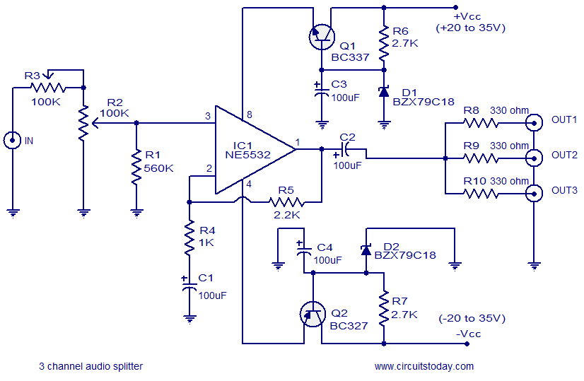
Here is the circuit diagram of a simple 3 channel audio splitter based on the IC NE5532. NE5532 is a dual internally compensated low noise opamp from Fairchild semiconductors. It has a high small signal and power bandwidth, making it well suitable for high quality audio applications.
Here the IC1 is wired as a non inverting amplifier with a gain 3.The audio signal to be splited is applied to the non inverting pin of IC1 through the POTs R2 and R3.Capacitor C2 works as a DC decoupler and resistors R8, R9, R10 splits the output of the IC1 into three channels. Components Q1, C3, R6, D1 forms a positive voltage regulator while components Q2, C4, R7, D2 forms a negative voltage regulator. If you have a +12/-12 V dual power supply, then the circuit can be directly powered from it and the regulator sections can be avoided.
Circuit diagram.
Notes.
- Assemble the circuit on a good quality PCB.
- Vcc can be anything between +/- 20 to35V DC
- IC1 must be mounted on a holder.
- Gain can be adjusted using the POTs R2 and R3.
- All capacitors must be rated at least 15V DC.


5 Comments
How can we use for stereo
Hey, you can use the other part of the Op Amp to make a second splitter ?, i.e. want to insert a left-right stereo signal and that this takes me 3 left and 3 right signals.
Another question, rather than the splitter is 3 channels I can add more resistance to this pull 4 channel?
Nice! One thing, is it necessary to use opamp with split pos & neg supplies? Or is it the nature of the RCA input that leads to split supplies?
Can we avoid pot R3 in this circuit.
R3 is used to limit the maximum setting of the input source not to over load at higher setting of R2. If you feel it is not required R3 can be deleted R2 alone can be used.