The bipolar junction transistor is the one which amplifies a small change in input current to produce a large change in output current. Another type of transistor, called a field effect transistor (FET), converts a change in input voltage into a change in output current and thus the gain of an FET is measured by its transconductance, defined as the ratio of change in output current to change in input voltage. The voltage is applied to the input terminal which is called its Gate and the current flowing through the transistor is depending on the electric field produced by the gate voltage. Under the gate electrode an insulating plate has been placed and so the gate current of an FET is approximately zero. Those FETs which uses a thin silicon dioxide as the insulator is known as the Metal Oxide Semiconductor (MOS) transistor or Metal Oxide Semiconductor Field Effect Transistor (MOSFET).
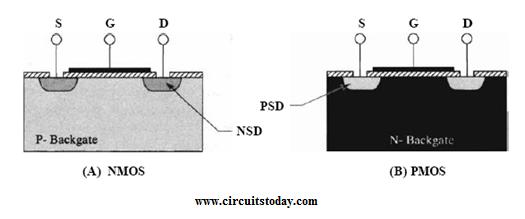
Based on the channel formed beneath the insulating layer, MOS transistors are classified as N-channel transistor (NMOS) and P-channel transistor (PMOS). A cross sectional view of both the transistors are shown in Fig 1. Each transistor should have a source, drain, gate and a backgate usually known as bulk terminal. In the case of an NMOS the source and gate are generated by diffusing N type dopant to a P substrate, and vice versa for PMOS. The source and drain of a MOS transistor are interchangeable and the carriers flow out of the source and come into the drain.
NMOS Transistors – Operation
The basic operation of an NMOS transistor is explained below. There are three regions of operation for a transistor.
- Cut off region (VGS < VTH)
- Triode region (VGS > VTH & VDS < VDSsat)
- Saturation region (VGS > VTH & VDS > VDSsat)
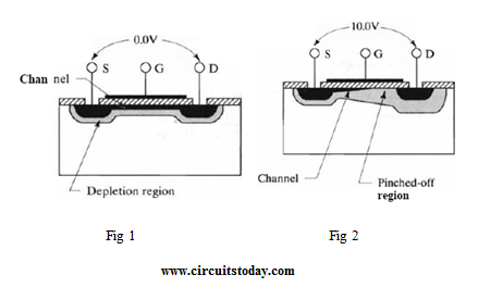
Initially consider the Tr with VGS =0, i.e. with no gate to source voltage is applied. It is similar to 2 diodes connected back to back between the source and the drain. So no current will flow from the source to drain. Also a depletion region will form at the source – substrate, drain – substrate junctions. When the VGS voltage is gradually increased below the threshold voltage (VTH), the holes under the gate are repelled to produce a depletion region, and it becomes continuous under the gate from source to drain. The VGS is then increased above the threshold voltage i.e. VGS > VTH. At this time the minority carriers (electrons) in the P sub crosses depletion region and reaches under the gate. This process is called inversion. The number of electrons reaches under the gate depends on the voltage VGS – VTH. Hence a conducting channel is produced because of this transverse electric field (Fig1). After the channel is established between the Source and the Drain, the VDS (Drain to source voltage) is increased gradually from 0. When the VDS become positive the Drain – Sub junction will get reverse biased and the depletion region here get widened as the drain becomes more positive with respect to the source (Fig2). Due to this lateral electric field, current flow starts from the source to drain and the current flow increases with the increase in the VDS. Hence the potential at the source is less than that at the source the depletion region widens near drain and the channel tapers here. At the point when VDS =VDSsat, the channel just touches the drain and the corresponding drain to source voltage is known as the pinch off voltage. Above the saturation voltage the current flow gets constant. Carriers move down the channel propelled by the relatively weak electric field along it. When they reach the edge of the pinched-off region, they are sucked across the depletion region by the strong electric field. The voltage drop across the channel does not increase as the drain voltage is increased; instead the pinched-off region widens. Thus, the drain current reaches a limit and ceases to increase.
Threshold voltage of MOS Transistor
The threshold voltage of a MOS transistor is the gate-to-source bias voltage required to just form a conducting channel with the backgate (bulk) of the transistor connected to the source. If the gate-to-source bias (VGS) is less than the threshold voltage, then no channel forms. The threshold voltage exhibited by a given transistor depends on a number of factors, including backgate doping, dielectric thickness, gate material, and excess charge in the dielectric. Each of these effects will be briefly examined.
Backgate doping has a major effect on the threshold voltage. If the backgate is doped more heavily, then it becomes more difficult to invert to create the channel. So a stronger electric field is required to achieve inversion, and the threshold voltage increases. The backgate doping of an MOS transistor can be adjusted by doing a shallow implant under the gate dielectric to dope the channel region. This type of implant is called threshold adjust implant (or VTH adjust implant).
Consider the effects of a VTH adjust implant upon an NMOS transistor. If the implant consists of acceptors, then the silicon surface becomes more difficult to invert and the threshold voltage increases. If the implant consists of donors, then the surface becomes easier to invert and the threshold decreases. If enough donors are implanted, the surface of the silicon can actually become counter doped. In this case, a thin layer of N-type silicon forms a permanent channel at zero gate bias. The channel becomes more strongly inverted as the gate bias increases. As the gate bias is decreased, the channel becomes less strongly inverted and at some point it vanishes.
The threshold voltage is also determined by the dielectric using beneath the gate electrode. A thicker dielectric weakens the electric field by separating the charges by a greater distance. Thus, thicker dielectrics increase the threshold voltage while thinner ones reduce it. Theoretically, the material of the dielectric also affects the electric field. In practice, almost all MOS transistors use pure silicon dioxide as the gate dielectric. Extremely thin layers of SiO2 can be fabricated with purity and uniformity. Alternate dielectric materials therefore are very rare in usage.
The gate electrode material also influences the threshold voltage of the transistor. While applying a voltage the electric field is produced by the difference in work functions between the gate and backgate materials. Most common, heavily doped polysilicon is using as the gate electrode. The work function of polysilicon can be varied to some extension by changing its doping. The presence of excess charges in the gate oxide or along the interfaces between the oxide and the polysilicon surface also a major factor that affects the threshold voltage. These charges may be ionized impurity atoms, trapped carriers, or structural defects. The presence of these charges will alter the electric field and thereby the threshold voltage. If the amount of trapped charge varies with time, temperature, or applied bias, then the threshold voltage will also vary.
The threshold voltage of this NMOS transistor is actually negative. Such a transistor is called a depletion-mode NMOS, or simply a depletion NMOS. In contrast, an NMOS with a positive threshold voltage is called an enhancement-mode NMOS, or enhancement NMOS. The majority of commercially fabricated MOS transistors are enhancement-mode devices, but there are a few applications that require depletion mode devices. A depletion-mode PMOS can also be constructed. Such a device will have a positive threshold voltage.
4 Comments
thanx