Earlier, I had explained two DIGITAL TO ANALOG CONVERTERS. Both of them have been designed for four inputs. But, if the number of inputs is more than four, the combination of output becomes more than 16. This makes the circuit more complex and the accuracy of the circuit reduces. Therefore, in critical and complex applications, a monolithic/hybrid D/A converter IC must be used. With the help of binary-weighted resistor, and R and 2R resistor methods, 8-bit,10-bit, 12-bit, 14-bit, and 16-bit D/A converters can be designed with a current output, voltage output, or both current and voltage outputs.
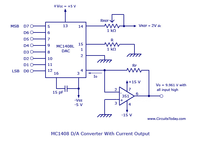
The most commonly used 8-bit D/A converter is MC 1408which has a current output that can be converted to a voltage type using a current to voltage converter op-amp. The design along with the current to voltage converter is shown in the figure below.
V0 = Vref/Rref *(RF)*{D7/2 + D6/4 + D5/8 + D4/16 + D3/32 + D2/64 + D1/128 + D0/256}
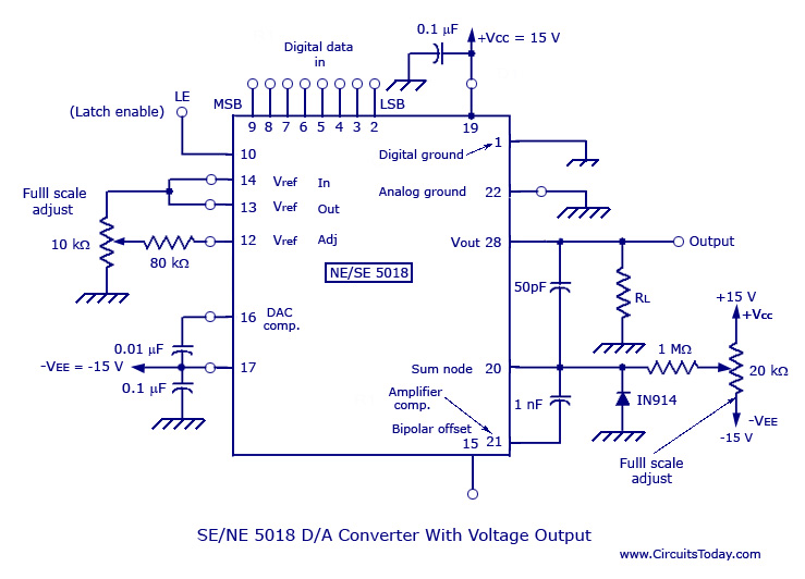
SE/NE 5018 is a typical 8-bit D/A converter with voltage output. The figure is shown below.
In the figure, the SE/NE 5018 circuit is configured for uni-polar output (0V to 10V). For 12 bits of resolution as well as current and voltage outputs, hybrid D/A converters such as DATEL DAC-H2 series is used.
For the correct selection of the D/A converter out of the lot, some important specifications of the converter must be known. They are explained below.
Specifications
- Resolution – It is determined by the number of input bits of the D/A converter. That is, an 8-bit converter has 28 possible output levels. Thus, its resolution is 1 part in 256. We can also say that resolution is the value of the LSB.
- Non-linearity or Linearity Error – It is the difference between the actual output of the DAC and its ideal straight line output. The error is normally expressed as a percentage of the full-scale range.
- Gain error and Offset Error – The deviations in the feedback resistor of the current to voltage resistor is the main reason for gain error, while, offset error implies that the output of the DAC is not zero when the binary inputs are all zero. This error stems from the input offsets (V and I) of the op-amp as well as of the DAC.
- Settling Time – The time needed for the DAC output to be within +/- 1/2LSB from zero to full scale input value is called settling time.
Applications
- Microcomputer interfacing
- CRT Graphics Generation
- Programmable Power Supplies
- Digitally controlled gain circuits
- Digital Filters


5 Comments
This site is one of the best sites on the Internet