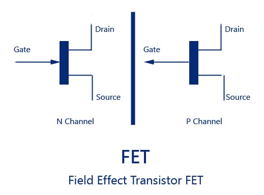
Introduction to FET-Field Effect Transistor
So far we have discussed the circuit applications of ordinary transistors, in which both holes and electrons take part. This is the reason that these are sometimes called the bipolar transistors. Such transistors have two main drawbacks namely low input impedance because of forward biased emitter junction and considerable noise level. Both of these drawbacks have been overcome, to a great extent in the field effect transistor (FET), which is an electric field (or voltage) controlled device. FET’s because of possessing all the advantages that tubes and ordinary transistors (BJTs) have, are replacing both the vacuum tubes and BJTs in applications.

A field-effect transistor (FET) is a three terminal (namely drain, source and gate) semiconductor device in which current conduction is by only one type of majority carriers (electrons in case of an N-channel FET or holes in a P-channel FET). It is also sometimes called the uni-polar transistor. Unlike a biploar transistor a FET requires virtually no input (bias signal) current and gives anextremely high input resistance -most important advantage over a BJT. Either BJT or FET devices can be used to operate in amplifier circuits or other similar electronic circuits, with different bias considerations.
There are two categories of FET’s namely:
1. Junction Field-Effect Transistors (abbreviated JFET’s or simply JFET’s). Please check the link for complete description.
2. Insulated-gate field-effect transistors (IGFETs), more commonly known as the metal-oxide semiconductor field-effect transistors (abbreviated MOSFETs or MOSTs).

Comments are closed.