Introduction to CMOS-Complimentary Metal Oxide Semiconductor FET’s
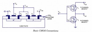
Complementary metal oxide semi-conductor devices are chips in which both P-channel and N-channel enhancement MOSFETs are connected in push-pull arrangement. The basic connections for CMOS are shown in figure.

Above figure shows various CMOS connections especially N-channel and P-channel CMOS connections.
In this circuit, two MOSFETs (P-channel MOSFET and N-channel-MQSFET) are connected in series so that source of P-channel device is connected to a positive voltage supply + VDD and the source of N-channel device is connected to the ground. Gates of both the devices are connected as a common input and drain terminals of both the devices are connected together as a common output.
When the input is kept low that is at 0 volt, then gate of MOSFET T, is at negative potential with respect to the source S1. So MOSFET T1 will be ON with its resistance RON = l kilo Ohm, while gate of MOSFET T2, will be at 0 Volt relative to its source. So T2 will be OFF with its resistance RSoff = 10^10 Ohms. Both of these resistances act like a potential divider and output of this will be approximately +VDD volts
In other case when the input is kept at high level that is +VDD volts then the gate of MOSFET T1, is at zero potential relative to the source, so T1 will be OFF with its resistance R0FF = 10^10 Ohms while gate of MOSFET T2 will be at positive potential relative to its source so the MOSFET T2 will be ON with its resistance RON = 1 Kilo Ohm. In this case output will be approximately 0 volt.

Above figure shows the CMOS output waveforms.
Except for a short time as the voltage drop from + VDD to zero or rises from zero to +VDD, the series combination of P-channel MOSFET (or PMOST) and N-channel MOSFET (or NMOS) has one transistor off with no current then drawn from the power supply. Thus the CMOS circuit operates with the input either high or low while drawing no power from the supply except during the brief time while switching between high and low output levels, when both transistors are ON as one is turning ON and the other is turning OFF. In fact, the power consumption of a CMOS circuit is zero at dc conditions, increasing as the applied signal frequency increases since the circuit is switching more often.
The CMOS device is used primarily in digital circuits, operating to provide output of either 0 V or + VDD (+ 5 V) while drawing very little power from the supply, Most low-power ICs (integrated circuits) are built-using CMOS transistors. Curve shown in figure gives relation between input and output voltages.
Advantage of CMOS
- The main advantage of CMOS is that the power dissipation is very small typically 50 nW.

Comments are closed.