Class B power amplifier.
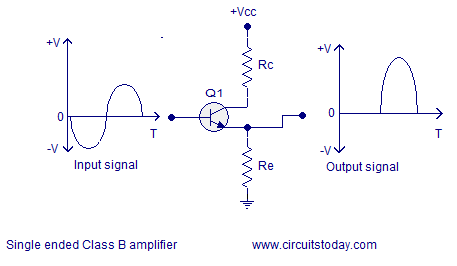
Class B amplifier is a type of power amplifier where the active device (transistor) conducts only for one half cycle of the input signal. That means the conduction angle is 180° for a Class B amplifier. Since the active device is switched off for half the input cycle, the active device dissipates less power and hence the efficiency is improved. Theoretical maximum efficiency of Class B power amplifier is 78.5%. The schematic of a single ended Class B amplifier and input , output waveforms are shown in the figure below.
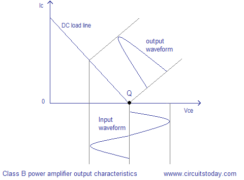
From the above circuit it is clear that the base of the transistor Q1 is not biased and the negative half cycle of the input waveform is missing in the output. Even though it improves the power efficiency, it creates a lot of distortion. Only half the information present in the input will be available in the output and that is a bad thing.Single ended Class B amplifiers are not used in present day practical audio amplifier application and they can be found only in some earlier gadgets. Another place where you can find them is the RF power amplifiers where the distortion is not a matter of major concern. Anyway, Class C amplifiers are more often used in RF power amplifier applications. Output characteristics of a single ended Class B power amplifier is shown in the figure below.One way to realize a practical Class B amplifier is to use a pair of active devices (transistors) arranged in push-pull mode where one transistor conducts one half cycle and the other transistor conducts the other half cycle. The output from both transistors are then combined together to get a scaled replica of the input. But there is a snag – there must be some way to split the input wave form to feed the individual transistors and there must be some way to put together the output of the individual transistors. Transformer coupling is solution for this problem and such amplifiers are called transformer coupled Class B amplifiers.
Transformer coupled Class B amplifier.
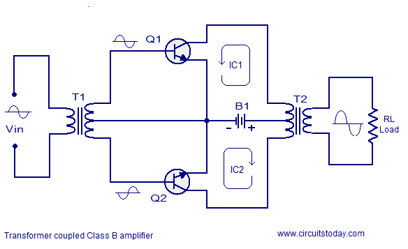
The circuit diagram of a simple transformer coupled class B power amplifier is shown in the figure above. Transistor Q1 and Q2 are the active elements. The transformer T1 reproduces the input signal into two copies which are 180° out of phase. From the above figure you can see that the transistor Q1 amplifies the positive half of the input signal and transistor Q2 amplifies the negative half of the input signal. Current flow path of the two transistors are also depicted in the above figure. The amplified two halves are joined together by the transformer T2. If an ideal transformer is used the DC components of the collector current of each transistors will flow in opposite directions through the transformer primary and they will cancel each other. That means there is no core saturation and there will be no DC components in the output.
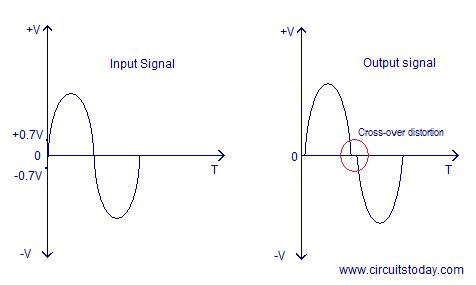
Since the transistors are not biased they remains OFF when there is no input signal and no current flows through the load. Each transistor starts conduction only when the amplitude of the input signal goes above the base-emitter voltage (Vbe) of the transistor which is about 0.7 V. This improves the efficiency but creates a problem called cross-over distortion.
Cross over distortion.
Since the active elements start conduction only after the input signal amplitude has risen above 0.7V, the regions of the input signal where the amplitude is less than 0.7V will be missing in the output signal and it is called cross over distortion. The schematic representation of cross-over distortion is shown in the figure below. In the figure, you can see that the regions of the input waveform which are under 0.7V are missing in the output waveform.
Advantages of Class B amplifier.
- High efficiency when compared to the Class A configurations.
- Push-pull mechanism avoids even harmonics.
- No DC components in the output (in ideal case).
Disadvantages of Class B amplifier.
- The major disadvantage is the cross-over distortion.
- Coupling transformers increases the cost and size.
- It is difficult to find ideal transformers.
- Transformer coupling causes hum in the output and also affects the low frequency response.
- Transformer coupling is not practical in case of huge loads.
Class AB power amplifier.
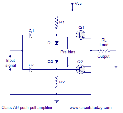
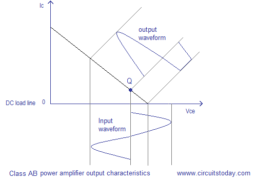 From the above figure it is clear that the Q-point is not positioned at cut-off unlike the Class B characteristics and there will be a small amount of collector current flowing at zero input. As a result, some part of the negative going half cycle will be also reproduced at the output. The amount of negative going half cycle reproduced at the output depends on the amount of pre-bias given to the transistor.
Practical Class AB power amplifier.
Advantages of Class AB power amplifier.
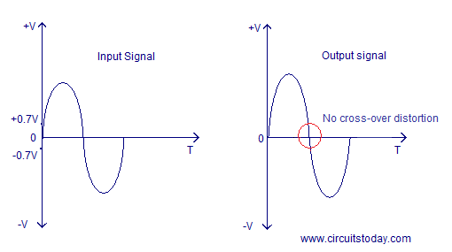
- No cross over distortion.
- No need for the bulky coupling transformers.
- No hum in the output.
Disadvantages of Class AB power amplifier.
- Efficiency is slightly less when compared to Class B configuration.
- There will be some DC components in the output as the load is directly coupled.
- Capacitive coupling can eliminate DC components but it is not practical in case of heavy loads.

Comments are closed.