An op-amp is usually used as a comparator in cases where its speed and accuracy are not critical. As illustrated in the earlier post (OP-AMP COMPARATOR), the switching speed of the op-amp comparator can be improved and noise can also be eliminated. The offset problems can also be reduced by adding a voltage compensating network and a offset reducing resistor. Since the op-amp is originally designed to act as an amplifier, its output will not act linearly with logic families like TTL. A TTL requires input voltages which range between (0-5) volts. Thus, to keep the op-amp’s output voltage swing between these ranges, other components like zener diodes are added onto the circuit. Such circuits with specified output swing are called voltage limiters.
Some of the most commonly used voltage limiter circuits are shown below.
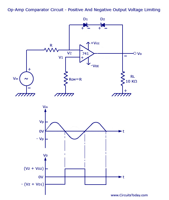
In the figure shown below, there are two zener diodes that are connected in the feedback path of the op-amp circuit. This design helps in keeping the voltage limit between the positive and negative values of the output voltage, V0. As shown in the waveform, as the voltage Vin increases from 0 to positive voltage, the value of V0 increases in the opposite direction (negative). This goes on until the diode D1 becomes forward biased and D2 goes into avalanche breakdown.

At this condition, V0 = VZ + VD1
VZ – Zener Voltage
VD1 – Voltage drop across D1 = 0.7V
If Vo increases from 0 to negative voltage, Vo increases positively until diode D2 is forward biased and D1 goes into avalanche condition.
A t this condition, V0 = VZ + VD2
VZ – Zener Voltage
VD1 – Voltage drop across D2 = 0.7V
Thus the limit of output voltage swing is between +(VZ + 0.7) and –(VZ + 0.7).
In the figure, ROM is used to reduce the offset problems. Vin will appear across resistor R, since the v1=v2=0V (virtual ground).
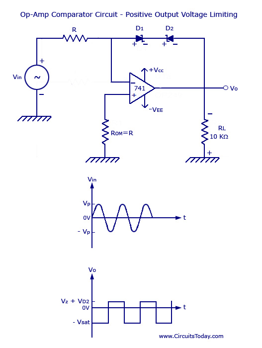
The figure below shows a combination of zener diode and rectifier diodes. This circuit is used to bring the level of swing of V0 to a positive direction.
When Vin ranges from 0 to positive voltage, D2 is reverse biased and thus V0 = -Vsat.
When Vin ranges from 0 to negative voltage, D2 is forward biased and D1 goes into avalanche condition. Thus V0 = VZ + VD2.

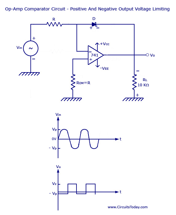
The figure below shows the use of a single zener diode in the feedback path of an op-amp. This enables the output to be limited between +VZ and –VD.
VZ – Zener Voltage
VD – Voltage drop across the forward biased zener.


5 Comments
respeced sir,
if my input voltage is 4.78v peak to peak and zener voltage is 4.78v then the output according to you will be having a positive peak of (4.78+0.7) and negative peak of -(4.78+0.7) then where the voltage is limited.this is my doubt so please clarify my doubt.can u mail me the answer plzzz
it is very bad the design of cir cit is not specified..
respected sir,
please give me a full description about VOLTAGE LIMITER CIRCUIT. and also give me a article on it.give me an information about, how can i make voltage limiter circuit at home for project…..with proper components which are used in it….please sir…help me…send all via on my e-mail which is ASILPATEL42@YAHOO.IN…..
thanks!!!
Excellent site information a very new
Wow! Am bless with the teaching. But can you tell me more about it application on real time, sorry for asking this question I love life application of electronics and I’m still a fresh student of electronics. Thanks.