Voltage Doubler and Inverter
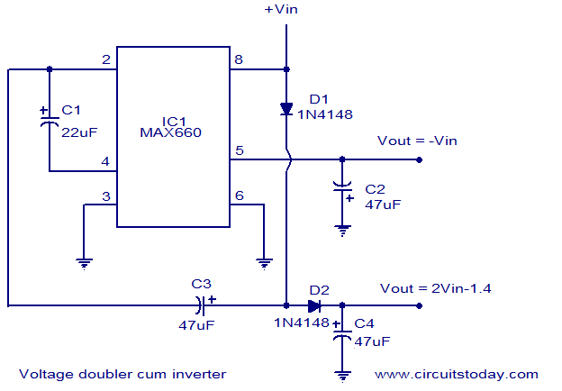
Given below is the circuit diagram of a DC Voltage doubler and voltage inverter. Circuit uses a voltage converter IC MAX660.
Description .
A voltage doubler cum inverter circuit using the IC MAX660 IC is shown here. MAX660 is a CMOS monolithic voltage converter IC from Maxim Semiconductors. The monolithic charge pump inverter circuitry inside the IC can invert +1.5V to 5.5V input to a corresponding negative output. The IC requires very few external components and can handle up to 100mA of load current.
In the circuit, voltage to be inverted is fed to the pin8 of MAX660 and inverted voltage will be available at pin5 of the same IC. Diodes D1, D2 and Capacitors C1, C3, C4 are related to the voltage doubler circuitry.
Circuit diagram of voltage doubler cum inverter:

Notes :
- The circuit can be assembled on a vero board.
- IC1 must be mounted on a holder.
- Capacitors are to be rated 15V.
- Vin can be anything between 1.5 to 5.5V DC.
- Load current must not exceed 100mA .
You may also be interested in other Power supply circuits in our website given below:
1. 10 Volts Switching Regulator
2. Simple DC Power Delay Circuit
4. Voltage Splitter using Op Amp
5. 12 Volts High Current Regulator
Take a look at our Power Supply Circuits category,if you would like to read more circuits and applications.

Comments are closed.