UJT relaxation oscillator
UJT relaxation oscillator is a type of RC ( resistor-capacitor) oscillator where the active element is a UJT (uni-junction transistor). UJT is an excellent switch with switching times in the order of nano seconds. It has a negative resistance region in the characteristics and can be easily employed in relaxation oscillators. The UJT relaxation oscillator is called so because the timing interval is set up by the charging of a capacitor and the timing interval is ceased by the the rapid discharge of the same capacitor. Before going into the details of UJT relaxation oscillator let’s have a look at the uni junction transistor (UJT).
UJT (uni junction transistor)
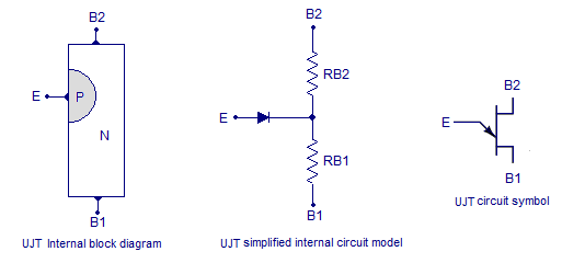
From the name itself, the UJT or uni junction transistor is a semiconductor device that has only one junction. The UJT has three terminals designated B1, B2 and E. The base material for a UJT is a lightly doped N-Type Silicon bar with ohmic contacts given at the lengthwise ends. These end terminals are called B1 and B2. Since the silicon bar is lightly doped, the resistance between B1 and B2 is very high (typically 5 to 10 KΩ). A heavily doped P-type region is constructed on one side of the bar close to the B2 region. This heavily doped P region is called emitter and it is designated as E. Resistance between E & B1 is higher than the resistance between E & B2 because E is constructed close to B2. The internal block diagram, simplified internal circuit model and circuit symbol of a UJT is given in the figure below.
The diode symbol shown in the internal circuit model represents the P-N junction formed between the heavily doped P-region (E) and the lightly doped N-Type bar.
UJT parameters
RBBO : It is the resistance between the terminals B1 and B2. In simple words, it is the resistance of the N-Type bar when measured lengthwise. If RB1 is the resistance of the bar from E to B1 and RB2 is the resistance of the bar from E to B2, then RBBO can be expressed as RBBO= RB1 +RB2. The typical range of RBBO is from 4KΩ to 10KΩ.
Intrinsic standoff ratio (η) : It is the ratio of RB1 to the sum of RB1 and RB2. It can be expressed as η = RB1/(RB1+RB2) or η = RB1/RBBO. The typical range of intrinsic standoff ratio is from 0.4 to 0.8.
UJT characteristics and circuit arrangement
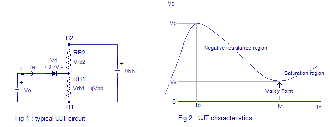
For ease of understanding, the internal model of the UJT is used in the circuit (Fig 1). B2 terminal of the UJT is made positive with respect to B1 terminal using the voltage source Vbb. Emitter terminal E of the UJT is forward biased using the voltage source Ve. Current starts flowing into the emitter only when the bias voltage Ve has exceeded the forward drop of the internal diode (Vd) plus the voltage drop across RB1 (Vrb1). This condition can be expressed using the following equation.
Ve = Vd + Vrb1
Considering the intrinsic stand off ratio η= RB1/(RB1+RB2), the equation becomes
Ve = Vd+ηVbb
A typical silicon diode has a forward voltage drop of 0.7V. When this factor is considered, the equation can be re written as
Ve = 0.7V + ηVbb
This minimum value of the emitter voltage Ve for which the emitter current starts to flow is called the firing voltage of UJT.
As the Ve is increased the emitter current Ie is also increased and the junction behaves like a typical P-N junction. But the Ve can be only increased up to a particular point called Vp (peak voltage). At this point a considerable amount of emitter current (Ie) flows and a significant number of holes are injected into the junction. These holes are repelled by B2 and attracted by B1. As a result, the region between emitter(E) and B1 terminal starts saturating by holes and the conductivity of this region starts to increase. This phenomenon of increasing conductivity by the insertion of holes is called conductivity modulation. This increased conductivity reduces RB1 and η. This results in a condition where emitter current Ie increases and the emitter voltage Ve decreases. This situation is similar to a negative resistance scenario. In the graph (Fig:2) you can see that the regions between Vp (peak voltage point) and Vv (valley voltage) have a negative slope. This negative resistance region in the UJT characteristics is employed in relaxation oscillators.
At last the emitter current Ie will be increased to a point that no more increase in conductivity is possible. This point is called “Valley point”. The emitter current corresponding to valley point is denoted as Iv and the corresponding emitter voltage is denoted as Vv. Beyond the valley point, the UJT is fully saturated and the junction behaves like a fully saturated P-N junction.
Applications of UJT
- Relaxation oscillators.
- Switching Thyristors like SCR, TRIAC etc.
- Magnetic flux sensors.
- Voltage or current limiting circuit.
- Bistable oscillators.
- Voltage or current regulators.
- Phase control circuits.
UJT relaxation oscillator
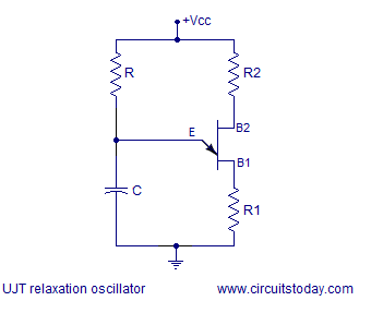
 The circuit diagram of a UJT relaxation oscillator is given shown above. R1 and R2 are current limiting resistors. Resistor R and capacitor C determines the frequency of the oscillator. The frequency of the UJT relaxation oscillator can be expressed by the equation F = 1/ (RC ln(1/(1-η)) where η is the intrinsic standoff ratio and ln stand for natural logarithm.
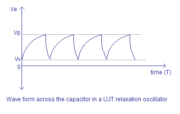
When power supply is switched ON the capacitor C starts charging through resistor R. The capacitor keeps on charging until the voltage across it becomes equal to 0.7V plus ηVbb. This voltage is the peak voltage point “Vp” denoted in the characteristics curve (Fig:2). After this point the emitter to RB1 resistance drops drastically and the capacitors starts discharging through this path. When the capacitor is discharged to the valley point voltage “Vv” (refer Fig : 1) the emitter to RB1 resistance climbs again and the capacitor starts charging. This cycle is repeated and results in a sort of sawtooth waveform across the capacitor. The saw tooth waveform across the capacitor of a typical UJT relaxation oscillator is shown in the figure below.
 Practical circuit diagram and testing of the UJT relaxation oscillator will be added soon.


14 Comments
Where do you get the period of oscillation Formula
Why and how B2 is made more +ve with respect to B1?
I am not able to understand how more proximity of emitter towards B2 makes it more +ve.
Why and how B@ is made more +ve with respect to B1?
I am not able to understand how more proximity of emitter towards B2 makes it more +ve?
Help on this question list four parameters that determines. the value of channel resistance in a JFET
i want to study theory working diagram of scr triggered by ujt relaxation full wave rectifier.
Hello
I am student of electrical engineering and i have read this passage,
Could anyone help me with this problem :
“When we reduce the RE in the image above the UJT remains switched on and we don’t have a oscillator anymore .”
do you know why this happens ?
Is that because equation written above for RE ? (the min and max for RE)
if it is so , what is the reason of remaining switched on !! it should be switched off
i am looking forward to hearing from you
thanks in advance
Hiiiiii………mohammadrezanargesi
m nt a scientist bt i thought of a small explanation……
the firing of UJT is related to the discharging time of the capacitor, while calculating the limiting value of discharging time u’l see it is independent of “Re”.
also for triggering UJT base/input voltage is significant which is again dependent on “C” and “R1″&”R2”.
hope m able to help u.
best of luck……
I’m also an electrical student the reason the UJT stays on is because you are not able to drop below the valley current which means you will never be able to shut the UJT down and it will always remain on. Good luck with engineering I’m only in my 3rd semester for a electrical technician.