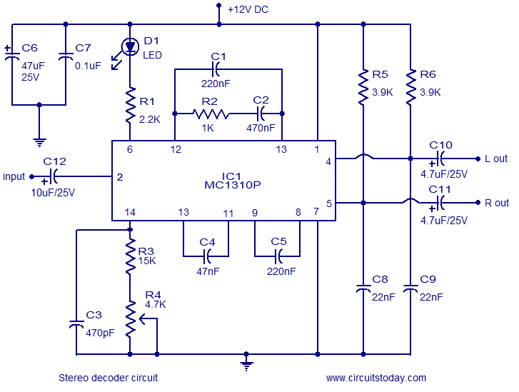
Stereo decoder circuit.
In FM stereo transmission left and right channels are algebraically encoded into sum (left + right) and difference (left-right) signals. This is done in order to make the mono FM receivers compatible with the stereo transmission. The mono receiver will reproduce the summed left and right channel and the listener will hear both these channels through a single loud speaker. Stereo decoder is a circuit which is used in stereo FM receivers in order to recover the left and right channel information from the composite transmission signal. This task is achieved by adding the difference signal to the summed signal to recover left channel and subtracting the difference signal from the summed signal to recover the right channel.
The circuit diagram of a stereo decoder using MC1310P IC from Motorola is shown below. MC1310P is an integrated stereo decoder IC chip which is available in 14 pin DIL plastic package.

Circuit description.
In the circuit composite signal if fed to the input pin (pin2) of the IC through decoupling capacitor C12. Capacitors C6 and C7 do the job of power supply filtering. Capacitor C3 plus Resistors R3 and R4 forms the RC for the ICs internal oscillator circuit. Resistor R2 plus capacitors C1 and C2 forms a loop filter. D1 is an indicator LED and R1 limits the current through it. The decoded left and right stereo outputs are available at pins 4 and 5 respectively. C10 and C11 are the DC decoupling capacitors for the left and right outputs.
Notes.
- The circuit can be assembled on a vero board or PCB.
- The circuit can be powered from anything between 8 to 14V DC.
- I recommend 12V DC for powering the circuit. Using a battery reduces noise and improves performance.
- Mount the IC on a holder.
- Voltage ratings of the electrolytic capacitors are shown in the circuit diagram.
- Input sensitivity is 1V RMS.
- Channel separation is 40dB and distortion is 0.3%.

4 Comments
Can i use lm1310 insted of mc1310
Can i use LM1310 in place of MC1310
is it working?
This site is a wealth scientific