Description.
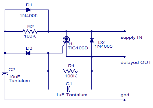
The circuit diagram shown here is of a simple DC power delay circuit that is based on an SCR. This circuit is a very handy one and can be employed in many applications. The working of this circuit is very simple. When the input power is applied the capacitor C2 charges through resistor R2 and when the voltage across the capacitor just exceeds the Zener diode D3’s breakdown voltage, it breaks down and the SCR H1 is triggered and the delayed power will be available at the delayed OUT terminal.
Circuit diagram.
Notes.
- The circuit must be assembled on a good quality PCB.
- The Zener diode must be rated half the input supply voltage.
- The current capacity of the circuit depends on the SCR and here it is 4A.


7 Comments
I build this circuit and it works fine. I do have some questions:
The role of R2 and C2 is clear. But what is the function of the other components?
* R1/C1?
* D2 ? I assume that this diode for the case the circuit that is powered is somehow inductive. In my case that is not the case. Can I take it out?
* D1?
Why is a thyristor used and not a plain transistor?
extra information are required of project details
Why when you say this is very simple, that you dont explain what C1,R1 and D2 do?
I presume that the zener is equal to the supply in. No comment was made about it.
Hi,..how to control the delay time?
How many seconds it can make delay
please reply…
Resistor R2 sets the delay by controlling the current that C2 uses to charge. Most likely, increasing the value of R2 will increase the delay time.
A potentiometer (variable resistor) could be useful for this.