Short Channel MOS Structures
This article discusses the different factors that limit the speed of a MOSFET. The common methods to reduce the parasitics like Scaled MOS (SMOS) and High-performance MOS (HMOS) is explained in detail with their structure and diagram.
There are many factors that limit the speed of a MOSFET. Because of the parasitic capacitances and resistances, the change in the channel current and output voltage occur slowly. This is due to the fact that when the input voltage at the gate input is changed, the parasitic capacitances must be either charged or discharged through a parasitic resistance. When the parasitics are greater, the charging or discharging become slower. The parasitic capacitances of diffusion regions against the gate and substrate namely, Cgd, Cgs, Cdb and Csb, have sufficient values. These parasitics can be reduced by the self-aligned gate structure.
The parasitics can also be reduced by scaling down of the dimensions. Some common methods are explained below.
1. Scaled MOS (SMOS)
The main purpose of scaling down the dimensions of a MOSFET with a metal gate or a silicon gate is that it will help in increasing the speed of the MOSFET and also reduces the power consumption. When a change in the speed and power consumption occurs the parasitic capacitances will also be reduced. But, for the appropriate working certain adjustments in the parameters must also be made. In particular, reduction of channel length, that is, the length between drain and source increases the speed because the transit time of the earners to cross the channel is reduced, and the parasitic capacitances are also reduced.
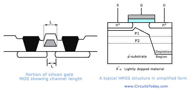
For a MOSFET to work properly, the channel length should nbe minimum. But if it is too short, thats is about 0.2 micro meters, the MOSFET will have certain complex physical phenomenons such as voltage breakdown, and punch through. The punch through causes current flow between source and drain without being controlled by the gate voltage. The minimum channel length in 1976 for depletion mode MOSFET was 6 micro meters which was brought down to 1.5 micro meters in 1982. This has reduced correspondingly the delay of a logic gate using MOS from 4 nano seconds to 0.2 micro seconds. It should be noted that for the sake of convenience, the horizontal length L of the silicon gate in the figure shown below is usually called channel length by the manufacturers because this length appears in a mask. In order to differentiate it from the real channel length L, this could be called a mask channel length. A scaled down n-MOS is usually called high-performance MOS (HMOS), as announced in 1977 by Intel and improved in later years.

2. High-Performance MOS (HMOS)
An HMOS device employs a single ion implantation to increase the doping level at the surface region of MOS. This method is employed so as to control the threshold voltage and increase the punch-through voltage. A double implanted HMOS as shown in the second figure above has p1 and p2 regions. The p1 region contains the threshold control implant, and the p2 region contains the punch-through control implant. By the use of these double implants, the HMOS with physically small-channel lengths can be used to minimise the effects occurring due to short channel. As the channel is shortened, departure from long- channel behaviour may occur as a result of a two dimensional potential distribution and high electric fields in the channel region.
The higher transfer conductance, in turn, leads to a larger voltage gain and gain-bandwidth product. Also, the drain current ID at any given gate voltage will be larger, so that the current- handling capability of the device is increased. Indeed, current ratings of up to 10 A are available with some
VMOS and vertical DMOS devices as discussed in the following posts.
TAKE A LOOK : DOUBLE-DIFFUSED MOS (DMOS)
TAKE A LOOK : V-GROOVE MOS (VMOS)

Comments are closed.