PLL FM demodulator.
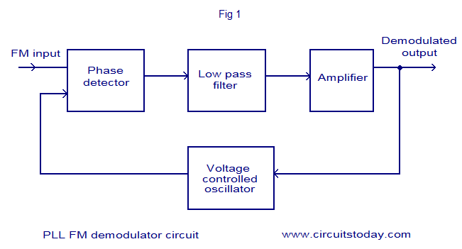
A simple PLL FM demodulator circuit using IC XR2212 is shown here. XR2212 is a highly stable, monolithic PLL (phase locked loop) IC specifically designed for communication and control system applications. The IC has 0.01 Hz to 300KHz frequency range, 4.5 to 20V operating voltage range, 2mV to 3Vrms dynamic range, high temperature range, TTL / CMOS compatibility and adjustable tracking range. The block diagram of a typical PLL FM demodulator circuit is shown below.

The working of a PLL FM demodulator is very easy to understand.The input FM signal and the output of the VCO is applied to the phase detector circuit. The output of the phase detector is filtered using a low pass filter, the amplifier and then used for controlling the VCO. When there is no carrier modulation and the input FM signal is in the center of the pass band (i.e. carrier wave only) the VCO’s tune line voltage will be at the center position. When deviation in carrier frequency occurs ( that means modulation occurs) the VCO frequency follows the input signal in order to keep the loop in lock. As a result the tune line voltage to the VCO varies and this variation is proportional to the modulation done to the FM carrier wave. This voltage variation is filtered and amplified in order to get the demodulated signal.
Circuit diagram.

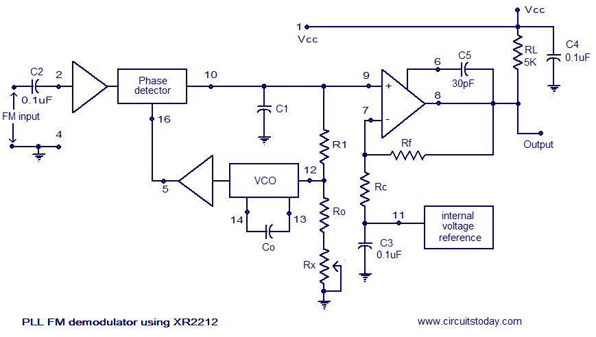
Composite FM signal is applied to pin 2 of the IC. Input impedance of this pin is around 20K and the voltage swing of the input signal must be between 10mV to 5V. Capacitor C5 is meant for frequency compensating the internal output opamp. The capacitor C5 is connected between pin 6 and 8 of the IC and its value can be 20 to 30pF. Co is the timing capacitor for the internal voltage controlled oscillator (VCO). The VCO frequency is inversely proportional to the value of the timing capacitor Co and its range can be 200pF to 10uF. C4 is the input supply by-pass capacitor. Free running frequency of the VCO is determined by the external timing resistor Ro. Value of Ro can be between 10 and 100K. Rx can used for fine tuning the VCO frequency. R1 and C1 forms a PLL loop filter. Resistors Rf and Rc sets the gain of the output amplifier section.
Design.
- Center frequency of the voltage controlled oscillator (VCO) , fo must be selected equal to the frequency of the FM carrier wave.
- Value of Ro can be in the range 10K to 100k and the recommended value is 20K.
- Co = 1/Rofo
- C1 = Co/4.
- Rf can be taken as 100K and RC can be taken as 80.6K for a +/-4V output swing.
- R1 can be taken as 89.3K.

2 Comments
thanks a lot
This All Are Very Usefull For Me,Thnks For This