The photoconductive cell is a two terminal semiconductor device whose terminal resistance will vary (linearly) with the intensity of the incident light. For obvious reasons, it is frequently called a photoresistive device.
The photoconductive materials most frequently used include cadmium sulphide (CdS) and cadmium selenide (CdSe). Both materials respond rather slowly to changes in light intensity. The peak spectral response time of CdS units is about 100 ms and 10 ms for CdSe cells. Another important difference between the two materials is their temperature sensitivity. There is large change in the resistance of a cadmium selenide cell with changes in ambient temperature, but the resistance of cadmium sulphide remains relatively stable. The spectral response of a cadmium sulphide cell closely matches thatof the human eye, and the cell is therefore often used in applications where human vision is a factor, such as street light control or automatic iris control for cameras.
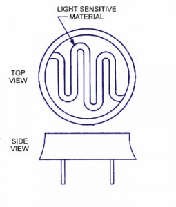
The essential elements of a photoconductive cell are the ceramic substrate, a layer of photoconductive material, metallic electrodes to connect the device into a circuit and a moisture resistant enclosure.
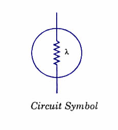
The circuit symbol and construction of a typical photoconductive cell are shown.


Light sensitive material is arranged in the form of a long strip, zigzagged across a disc shaped base with protective sides. For added protection, a glass or plastic cover may be included. The two ends of the strip are brought out to connecting pins below the base.
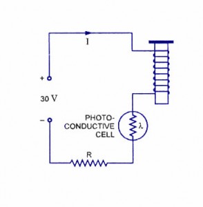
Photoconductive cell circuit:

Characteristics of a Photoconductive cell:

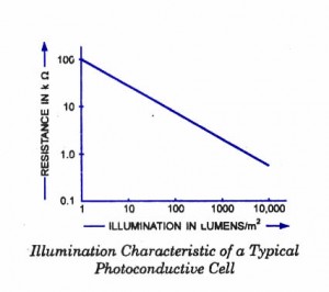
The illumination characteristics of a typical photoconductive cell are shown from which it is obvious that when the cell is not illuminated its resistance may be more than 1 00 kilo ohms. This resistance is called the dark resistance. When the cell is illuminated, the resistance may fall to a few hundred ohms. Note that the scales on the illumination characteristic are logarithmic to cover a wide ranges of resistance and illumination that are possible. Cell sensitivity may be expressed in terms of the cell current for a given voltage and given level of illumination.
The major drawback of the photoconductive cells is that temperature variations cause substantial variations in resistance for a substantial variations in resistance for a particular light intensity. Therefore such a cell is unsuitable for analog applications.
The photoconductive cell used for relay control is shown as circuit above When the cell is illuminated, its resistance is low and the relay current is at its maximum. When the cell is dark, its high resistance reduces the current down to a level too low to energize the relay. Resistance R is included to limit the relay current to the desired level when the resistance of the cell is low. Photoconductive cells are used to switch transistors on and off, as illustrated in figure. When the cell shown in figure is dark, the transistor base is biased above its emitter level, and the device is turned on. When the cell is illuminated, the lower resistance of the cell in series with R biases the transistor base voltage below its emitter level. Thus, the device is turned off.

7 Comments
I think this is one of the most significant information for me. And i am glad reading your article. But want to remark on some general things, The web site style is wonderful, the articles is really nice : D. Good job, cheers