Introduction to Operational Amplifiers
In this post, the basics of an operational amplifier (generally abbreviated as op-amp) will be analysed along with its block diagram, basic structure, symbol, types and a detailed explanation of the typical op-amp.
What is an operational amplifier (op-amp)?
An op-amp is a multi-stage , direct coupled, high gain negative feedback amplifier that has one or more differential amplifiers and its concluded with a level translator and an output stage.A voltage-shunt feedback is provided in an op-amp to obtain a stabilized voltage gain. Op-amps are available as Integrated Circuits (IC’s).
The main use of an op-amp is to amplify ac and dc input signals and was initially used for basic mathematical operations such as addition, subtraction, multiplication, differentiation and integration. Nowadays , the application of op-amp’s varies from ac and dc signal amplification to use in active filters, oscillators, comparators, voltage regulators, instrumentation and control systems, pulse generators, square wave generators and many more electronic circuits. For the design of all these circuits the op-amp’s are manufactured with integrated transistors, diodes, capacitors and resistors, thus making it an extremely compact, multi tasking, low cost, highly reliable and temperature stable integrated circuit. It is also designed in such a way that the external characteristics can be changed with the addition of external components like capacitors and resistors. Thus it can act as a complete amplifier with various characteristics.
Block Diagram Of Operational Amplifier (Op-amp)
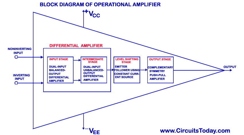
The block diagram of a multi-stage operational amplifier is given below.
The op-amp begins with a differential amplifier stage, which operates in the differential mode. Thus the inputs noted with ‘+’ & ‘- ‘ . The positive sign is for the non-inverting input and negative is for the inverting input. The non-inverting input is the ac signal (or dc) applied to the differential amplifier which produces the same polarity of the signal at the output of op-amp. The inverting signal input is the ac signal (or dc) applied to the differential amplifier. This produces a 180 degrees out of phase signal at the output.
The inverting and non-inverting inputs are provided to the input stage which is a dual input, balanced output differential amplifier. The voltage gain required for the amplifier is provided in this stage along with the input resistance for the op-amp. The output of the initial stage is given to the intermediate stage, which is driven by the output of the input stage.In this stage direct coupling is used, which makes the dc voltage at the output of the intermediate stage above ground potential. Therefore, the dc level at its output must be shifted down to 0Volts with respect to the ground. For this, the level shifting stage is used where usually an emitter follower with the constant current source is applied. The level shifted signal is then given to the output stage where a push-pull amplifier increases the output voltage swing of the signal and also increases the current supplying capability of the op-amp.
Symbol Of Operational Amplifier (Op-amp)
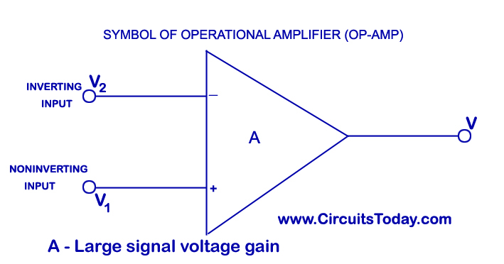
The schematic symbol of an op-amp is shown below.
The above shown symbol is the most widely used op-amp symbol for all electronic circuits.
V1 (Volts) – Non-inverting input voltage.
V2 (Volts) – Inverting input voltage.
V0 (Volts) – Output voltage
Characteristics Of Operational Amplifiers (Op-amp)
1. High input impedance- More than 100kilo ohms.
2. Low output – Less than 100 ohms.
3. Amplifier signals with frequency range from 0Hz to 1MHz.
4. Low offset voltage and low offset current.
5. Very high voltage gain – About 2,00,000.
Basic operational amplifier circuits
As explained earlier differential circuits are one of the most basic circuitry used in op-amp’s. We have already explained differential amplifier and its working in an earlier post. You can check the links here – Differential Amplifier.
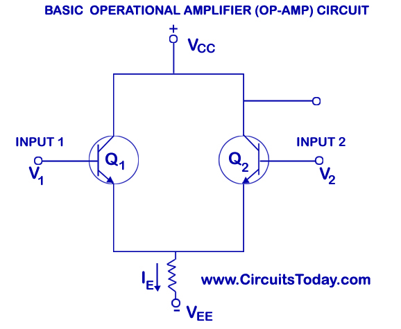
Shown below is a differential amplifier circuit that is modified to use an op-amp. This constitutes the basic op-amp circuit and explains about the input characteristics of a typical op-amp IC.
The basic configuration of the circuit is drawn above. Two transistors Q1 and Q2 are provided, in which the input is provided to the base of both the transistors. Both the transistor emitters are connected to a common emitter RE so that the two input signals are affected by either or both input signals. Two supply voltages VCC and VEE are connected to both the collectors and emitters QI and Q2. In the circuit diagram, there is no indication of common ground point. It must be understood that the opposite points of both positive and negative voltage supplies are connected to the ground.
When input at point 1(V1) increases , the emitter current of transistor Q1 increases, and thus causes an increase of voltage at top of the emitter resistance RE. Thus it decreases the base-emitter voltage VBE of transistor Q2. Thus, when VBE of Q2 decreases, there is less current flow in the transistor Q2.This brings a voltage drop in the collector resistance RC and an increase in the output voltage VOUT as it is the difference between the collector supply voltage VCC and voltage drop in collector resistance RC (ICRC).This brings us to the conclusion that there is will be an increase in output voltage when there is an increase in input voltage V1. This why V1 is considered as the non-inverting input. Vout is in phase with V1.
In another instant, when the voltage V2 increases, the collector current of Q2 increases, and makes way for a voltage drop in collector resistance and thus a decreased output voltage VOUT. This is why V2 is considered as the inverting input. VOUT is 180 degrees out of phase with V2.
A basic introduction of uA741 op-amp has already been given. Check out the link below.
The article mainly describes what an op-amp is., the op-amp symbol, the concept of the inverting and non-inverting input, and many more. It also describes about the popularity of th 741 IC, among th different types of op-amps available in the market. The op-amp features, and the need for dual power supply for the IC is also explained . You can understand more about the packaging style, and the op-amp pin assignment along with the different ratings of an ideal op-amp 741 IC. Some of the basic applications of an op-amp are listed below. Check out the detailed description by clicking on the main links.
The circuit diagram and the working of an op-amp as a comparator are shown in the article. There are mainly two types of comparators. One is the inverting comparator circuit, and the other is the non-inverting comparator. Both of them are explained with neat waveforms, and the different applications of the circuit are also given.
The application of op-amp as a fast operating voltage level detector is shown in this main article with the help of a circuit diagram and its corresponding waveform. The exact working of the circuit is also explained with the equations of the different reference voltages when the output is positively saturated and negatively saturated. The different characteristics of the schmitt trigger is also explained along with its UTP and LTP.
Astable Multivibrator Using Op-amp
The working of op-amp as a square wave generator is explained with the help of a circuit diagram and waveform. The output voltage equation, and the capacitor charging equation is also given. The reason for calling the circuit a “free-running multivibrator” is also explained.
The basics of pulse generator is explained in this post. The circuit diagram and waveform is illustrated in the article along with the steady state conditions and capacitor voltage equations.
This is an applied form of an op-amp comparator circuit. Here the reference voltage is made zero. The zero crossing detector using inverting op-amp comparator is explained with a circuit diagram and waveform.
A voltage divider circuit is connected to the non-inverting input of an op-amp. The circuit is explained in detail in the original post.


Comments are closed.