NMOS Fabrication Process
In this article the various steps needed for NMOS Fabrication are explained in detail along with diagrams.
To know the basic IC Fabrication Techniques, click on the link below.
TAKE A LOOK : IC FABRICATION TECHNIQUES
There are a large number and variety of basic fabrication steps used in the production of modern MOS ICs. The same process could be used for the designed of NMOS or PMOS or CMOS devices. The gate material could be either metal or poly-silicon (as described in this article for NMOS device). The most commonly used substrate is bulk silicon or silicon-on-sapphire (SOS). Inorder to avoid the presence of parasitic transistors, variations are brought in the techniques that are used to isolate the devices in the wafer.
This post describes the silicon-gate process. The important distinguishing characteristics of such structure will be described later.
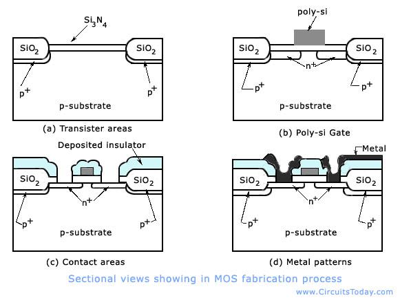
The fabrication sequence of n-channel MOS IC is shown in the figure below.

NMOS Fabrication Steps
- By the process of Chemical Vapour Deposition (CVD), a thin layer of Si3N4 is deposited on the entire wafer surface. With the first photolithographic step, the areas where the transistors are to be fabricated are clearly defined. Through chemical etching, Si3N4 is removed outside the transistor areas. In order to suppress the unwanted conduction between transistor sites, an impurity such as Boron is implanted in the exposed regions. Next, SiO2 layer of about 1 micro meters thickness is grown in these inactive, or field regions by exposing the wafer to oxygen in an electric furnace. This is known as selective or local oxidation process. The Si3N4 is impervious to oxygen and thus inhibits growth of the thick oxide in the transistor regions.
- Next, the Si3N4 is removed by an etchant that does not attack SiO2. A layer of oxide about 0.1 micro meters thick is grown in the transistor areas. Then a layer of poly-Silicon is grown over the entire wafer by CVD process. The second photolithographic step shows the desired patterns for gate electrodes. The unwanted poly-Silicon is removed by chemical or plasma etching. In order to introduce a source and drain in particular regions for the MOS device, an n-type dopant, such as phosphorus or arsenic, is introduced. This is done by either Diffusion or Ion Implantation method. The thick field oxide and the poly- silicon gate are barriers to the dopant, but in this process, the poly-Si becomes heavily n-type.
- Again, through CVD process, an insulating layer, SiO2, is deposited. As shown in the figure above, the third photolithographic step shows the areas in which contacts to the transistors are to be made. Chemical or plasma etching selectively exposes bare silicon or poly-Si in the contact areas.
- Al is used for the interconnection. As shown in the figure above, the fourth masking step shows the Al as desired for the circuit connections.
The final steps of the process are identical to those described for bipolar transistor ICs. Above process is the simplest possible. For advanced processing of NMOS and CMOS, 7 to 12 masking steps are required.

4 Comments
Awesome Article, Thanks Sir this topic was quite difficult to understand thanks for easy explanation.
Hope to learn more from here!
very nice concept
good explaination…
Very nice post….