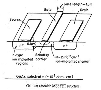
The figure below shows a diagram of gallium arsenide (GaAs) MESFET (metal-semiconductor field-effect transistor). MESFET is nothing but a JFET fabricated in GaAs which employs a metal-semiconductor gate region (a Schottky diode). The device operates in essentially the same way as does a junction-gate FET, except that instead of a gate-channel on junction there is a gate-channel Schottky barrier. The depletion region associated with this barrier will control the effective height of the conducting channel and can thereby control the drain-to-source current of the device.

The width of this depletion region will increase with increasing gate voltage so that we see again that the gate will be the control electrode and as long as the Schottky barrier is reverse biased, the gate current will be very small.
Electron mobility in GaAs (8500 cm2/v-s) is much higher than that of silicon and allows MESFET operation at frequencies higher than can be achieved with silicon devices. The MESFET also possesses very short channel length. This results in very short channel transit times for electrons. As a result, MESFET can operate well into the range of 1 to 10 gigahertz (GHz). Thus, applications of MESFETs were initially in microwave circuits for high frequency performance.
However, since 1984, high-speed logic circuits employing MESFETs have been produced commercially.
These logic circuits are made compatible with the high-speed bipolar logic family called emitter-coupled logic (EGL).

10 Comments
Youre so cool! I dont suppose Ive read anything like this before. So nice to search out somebody with some unique ideas on this subject. realy thanks for beginning this up. this website is one thing that is wanted on the internet, somebody with a bit originality. helpful job for bringing one thing new to the internet!