A digital system is basically a binary world. One where the language is restricted to 1s and 0s. Therefore, to make the best of these 1s and Os, logic gates form the foundation to build a digital system that we know today. Hence, if you are keen on understanding digital electronics, you must be clear with the basic boolean logic.
This article is all about logic gates and their types. It aims to be a stepping stone for all the digital electronics enthusiasts who are embarking on their learning journey. Some of the common examples of the application of digital logic gates are half adder, full adder, and flip flops.
What are digital logic gates?
Digital logic gates are simply a string of transistors working together to solve basic boolean functions. A logic gate is considered as a device that has the ability to produce one output level with the combinations of input levels. Logic 1 represents high, and logic 0 represents low. Here various combinations of binary mathematical functions are applied to show the true state of a digital system.
Working of Logic Gates
The reason for which the computers are capable of performing complex operations is due to the interconnection of these logic gates. Logic gates are implemented by using transistors, diodes, relays, optics, and molecules or even by several mechanical elements. Due to this reason, the logic gates can also be considered electronic circuits. The logic gates can be built up in a wide variety of forms such as large-scale integrated circuits (LSI), very large-scale integrated circuits (VLSI), and also in small-scale integrated circuits (SSI). Here the inputs and output of all the gates of integrated devices can be accessed and also the external connections are made available to them just like discrete logic gates.
The two logic levels
Inputs and outputs of logic gates are in two levels termed as HIGH and LOW, or TRUE and FALSE, or ON and OFF, or simply 1 and 0. A table that lists out the combination of input variables and the corresponding output variables is termed as “TRUTH TABLE”. It explains how the logic circuit output responds to various combinations of logic levels at the inputs. Here we are following level logic, in which the voltage levels are represented as logic 1 and logic 0. Level logic is of two types such as positive logic or negative logic.
In the positive logic system, the higher of the two voltage levels are represented as 1, and the lower of the two voltage levels are represented as 0. But in the negative logic system, the higher of the two voltage levels are represented as 0 and the lower of the two voltage levels are represented as 1. While considering the transistor-transistor logic (TTL), the lower state is assumed to be zero volts (0V), and the higher state is considered as five volts positive (+5V).
What are the types of digital logic gates?
There are mainly 7 types of logic gates that are used in expressions. By combining them in different ways, you will be able to implement all types of digital components. Let’s dig deep into each of the basic logic gates and their operation.
There are seven basic types of logic gates:
AND GATE
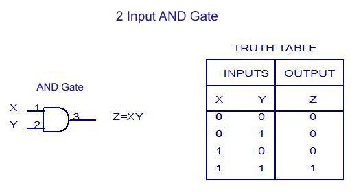
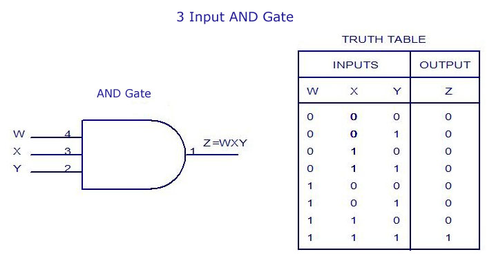
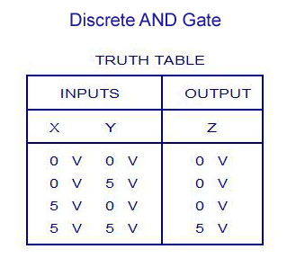
An AND gate requires two or more inputs and produces only one output. The AND gate produces an output of logic 1 state when each of the inputs are at logic 1 state and also produces an output of logic 0 state even if any of its inputs are at logic 0 state. The symbol for AND operation is ‘.’, or we use no symbol for representing. If the inputs are of X and Y, then the output can be expressed as Z=XY. The AND gate is so named because, if 0 is called “false” and 1 is called “true,” the gate performs in the same way as the logical “and” operator. The AND gate is also named as all or nothing gate. The logic symbols and truth tables of two-input and three-input AND gates are given below.
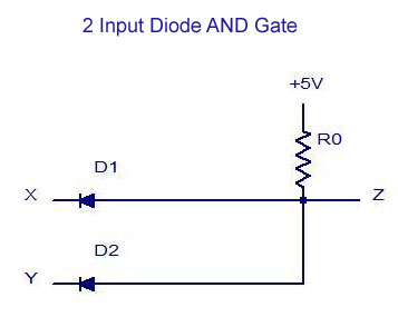
Discrete AND gates may be realized by using diodes or transistors. The inputs represented as X and Y may be either 0V or +5V correspondingly. The output is represented by Z . In the diode of AND gate, when both the inputs are of same value, X=+5V and Y= +5V, then the diodes are in OFF condition. As a result, no current flows through the resistor and there will not be any voltage drop across the resistor. Here the output will be Z=+5V. Similarly, when both the inputs such as X and Y are equal to 0V, then the corresponding diodes such as either D1 or D2 or both the diodes are at ON state and act as short circuits. Here the output will be Z corresponds to 0V. In practical cases the output z corresponds to 0.6V or 0.7V, which is treated as logic 0 state.
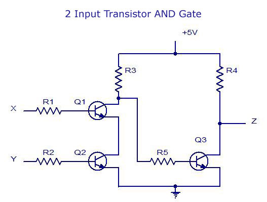
In the case of transistor AND gate, When the inputs X, Y = 0V or when X=0V and Y= +5V or when X=+5V and Y=0V, both the transistors Q1 and Q2 are at OFF state. At the same time, Transistor Q3 gets enough base drive from the supply through Resistor R3 and so transistor Q3 will be ON. Thereby the output voltage Z= Vce(sat) corresponds to 0V. When both the inputs are equal to +5V, the transistors Q1 and Q2 will be ON and therefore the voltage at the collector of transistor Q1 will drop. Due to this the transistor Q3 doesn’t get enough base drive and turns OFF. As a result no current flows through the collector resistor of Q3 and , thereby no voltage drop across it. So the final output voltage corresponds to +5V. The truth table for this gate circuit is shown below:
Applications of AND gate
One of the most common applications of AND gate is as an enabling gate in a circuit. As an enabling gate, AND gate allows data to process through a channel, like in a frequency measuring circuit of a pulsed waveform. Here a gating pulse of known frequency acts as an input to the AND gate, while the second input corresponds to the known frequency pulse. As both of them are compared, only the unknown frequency pulse is allowed to pass through the gate. The output acts as the clocked input to the frequency counter circuit.
OR GATE
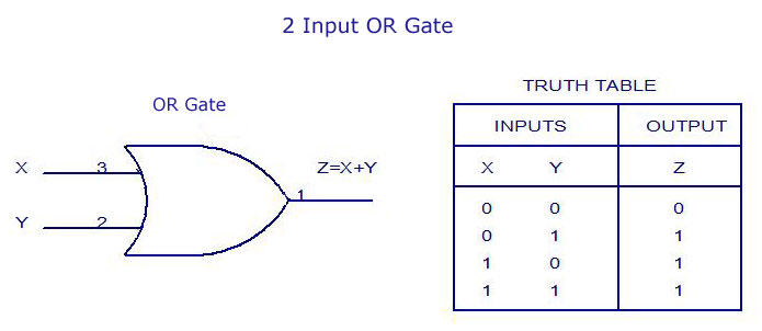
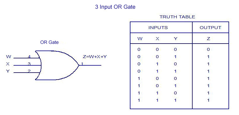
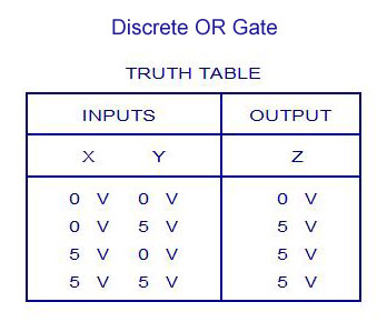
Similar to AND gate, an OR gate may also have two or more inputs but produce only one output. The OR gate produces an output of logic 1 state even if any of its inputs is in logic 1 state and also produces an output of logic 0 state if any of its inputs is in logic 0 state. The symbol for OR operation is ‘+’. If the inputs are of X and Y, then the output can be represented as Z=X+Y. An OR gate may also be defined as a device whose output is 1, even if one of its input is 1. OR gate is also called as any or all gate. It is also called as an inclusive OR gate because it consists of the condition of ‘both the inputs can be present’. The logic symbols and truth table for two-input and three-input OR gates are given below.
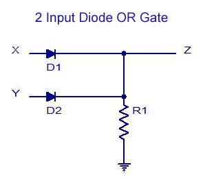
Discrete OR gates may be realized by using diodes or transistors. The inputs represented as X and Y may be either 0V or +5V correspondingly. The output is represented by Z . In the diode of OR gate, when both the inputs are of same value, X=0V and Y= 0V, then both the diodes are in OFF condition. As a result, no current flows through the resistor and there will not be any voltage drop across the resistor. Here the output will be Z=0V. Similarly, when both the inputs or either the inputs such as X and Y are equal to +5V, then the corresponding diodes either D1 or D2 or both the diodes are at ON state and act as short circuits. Here the output will be Z corresponds to +5V. In practical cases the output Z corresponds to +5V-diode drop = +5V – 0.7V = +4.3V, which is regarded as Logic 1 state.
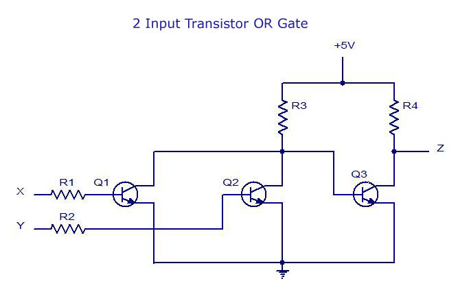
In the case of transistor OR gate, when the inputs X=0V and Y = 0V both the transistors Q1 and Q2 are at OFF state. At the same time, Transistor Q3 gets enough base drive from the supply +5V through Resistor R3 and so transistor Q3 will be ON. Thereby the output voltage Z= Vce(sat) corresponds to 0V. When either the inputs X and Y or both the inputs are equal to +5V, then the corresponding transistors either Q1 or Q2 will be ON or both the transistors Q1 and Q2 will be ON and therefore the voltage at the collector of transistor Q1 is VCE(sat) corresponds to 0V. Due to this reason the transistor Q3 doesn’t forward bias the base-emitter junction and turns OFF. So the final output voltage corresponds to +5V (logic 1 state). The truth table for this gate circuit is shown below:
Applications of OR GATE
OR gate is used in circuits in which the occurrence of one or more than one event is to be detected. One common example of this can be a temperature detector in an industrial unit.
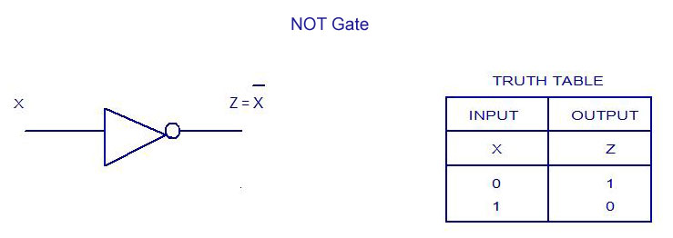
NOT GATE
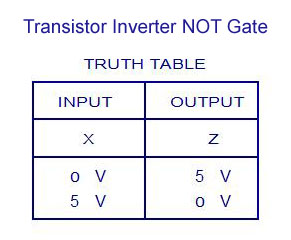
The NOT gate is also called an inverter, simply because it changes the input to its opposite. The NOT gate is having only one input and one corresponding output. It is a device whose output is always the complement of the given input. That means the NOT gate produces an output of logic 1 state when the input is of logic 0 state and also produces the output of logic 0 states when the input is of logic 1 state. The NOT operation is denoted by ’-‘(bar). When the input variable to the NOT gate is represented by ‘X’ and the output is represented by ‘Z’. In the NOT operation it can be read as ‘Z is equal to X bar’. The logic symbol and truth table are given below:
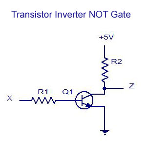
Discrete NOT gate may be realized by using transistors. The inputs represented as X may be either 0V or +5V correspondingly. The output is represented by Z. When the input X = 0V, then the transistor Q1 will be reverse biased and therefore it remains OFF. As a result no current flows through the resistor and thereby there will not be any voltage drop across the resistor. As a result, the output voltage Z corresponds to +5V. When the input X= +5V, transistor Q1 is ON and the output voltage Z=V ce(sat) corresponds to 0V. The truth table for the NOT gate is given below:
Applications of NOT Gate
Since NOT gates invert the input signal, and consume low power, these are used as an inverter within certain circuits. One common application of this kind of inverter is in square wave oscillators that usually produce clock input.
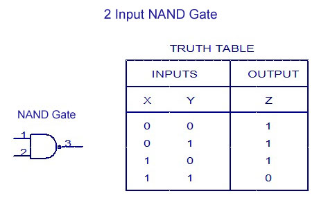
NAND GATE
The NAND and NOR gates are the universal gates. Each of these gates can realize the logic circuits single-handedly. The NAND and NOR are also called universal building blocks. Both NAND and NOR have the ability to perform three basic logic functions like AND, OR, and NOT. NAND gate is a combination of an AND gate and a NOT gate. The expression for the NAND gate is ‘—‘whole bar. The output of the NAND gate is at logic 0 level only when each of the inputs assumes a logic 1 level. The truth table of the two-input NAND gate is given below:
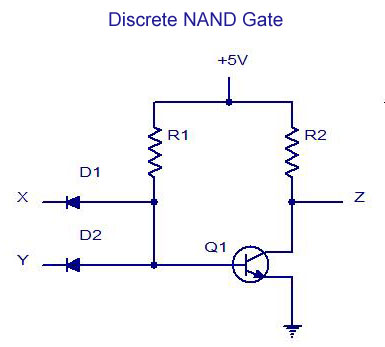
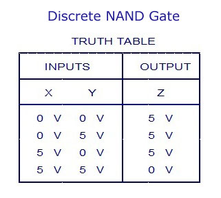
A Discrete two-input NAND gate is as shown in the figure. The two inputs are represented by X and Y. The output is represented by Z . When the input X and Y= +5V, then both the diodes D1 and D2 are OFF. The transistor Q1 gets enough base drive from the supply through resistor and therefore transistor Q1 is ON and the output Z=Vce(sat) corresponds to 0V. Similarly when inputs either x=0V or Y=0V or when both inputs are equal to 0V, at that time the transistor Q1 is OFF and therefore, output voltage Z= +5V. The truth table is given below:
Applications of NAND Gate
NAND gate is known as universal gate and can be found in many circuits. Most common of the lot are burglar alarms, and alarms.
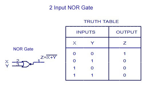
NOR GATE
NOR means NOT OR. That means, NOR gate is a combination of an OR gate and a NOT gate. The output is logic 1 level, only when each of its inputs assumes a logic 0 level. For any other combination of inputs, the output is a logic 0 level. The truth table of two-input NOR gate is given below:

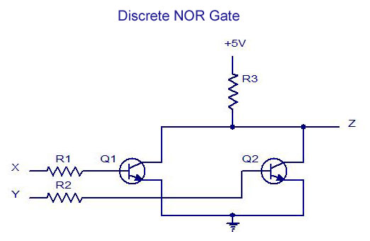
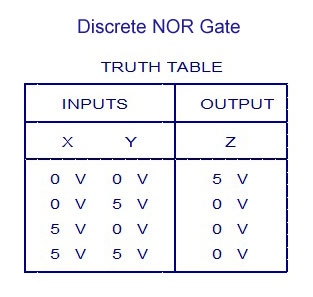
Discrete two-input NOR gate is as shown in the figure. The inputs represented as X and Y may be 0V correspondingly. As a result the transistors Q1 and Q2 are OFF, as a result no current flows through the resistor and thereby there will not be any voltage drop across the resistor. Here, the output voltage Z corresponds to +5V. When either of the input X= +5V or Y=+5V or both the inputs corresponds to +5V, the corresponding transistor Q1or Q2 or both Q1 and Q2 are ON . Therefore the output voltage Z=V ce(sat) corresponds to ground and equal to 0V. The truth table for the NOR gate is given below:
Applications of NOR Gate
Just like NAND gate, NOR gate can be used to build every other logic gate and hence these two are called universal gate. One of the common application is in combinational circuits like the adder and subtractor circuits.
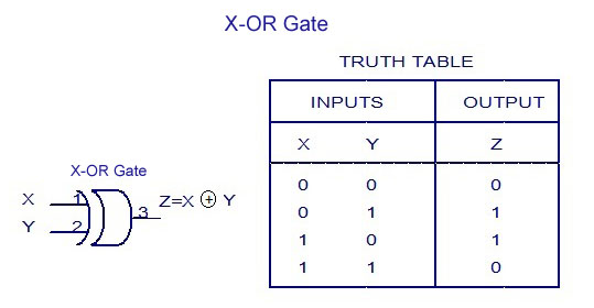
EXCLUSIVE-OR GATE (X-OR) GATE
An X-OR gate is a two-input, one output logic circuit. X-OR gate assumes a logic 1 state when any of its two inputs assumes a logic 1 state. When both the inputs assume the logic 0 state or when both the inputs assume the logic 1 state, the output assumes a logic 0 state. The output of the X-OR gate will be the sum of the modulo sum of its inputs. X-OR gate is also termed an anti-coincidence gate or inequality detector. An X-OR gate can also be used as an inverter by connecting one of the two input terminals to logic1 and also by inputting the sequence to be inverted to the other terminal.
Applications of X-OR gate
The simplest application of X-OR gate is to create arithmetic operations circuit or as a parity checker. They can also be used in controlled inverter circuits as well.
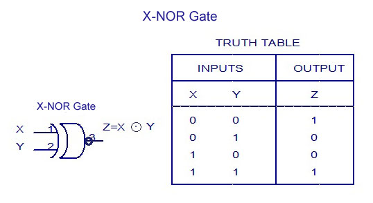
EXCLUSIVE-NOR (X-NOR) GATE
An X-NOR gate is a combination of an X-OR gate and a NOT gate. The X-NOR gate is also a two-input, one output concept. The output of the X-NOR gate will be logic 1 state when both the inputs assume a 0 state or when both the inputs assume a 1 state. The output of the X-NOR gate will be logic 0 state when one of the inputs assumes a 0 state and the other a 1 state. It is also named a coincidence gate, because its output will be 1 only when the inputs coincide. X-NOR gate can also be used as an inverter by connecting one of the two input terminals to logic 0 and also by inputting the sequence to be inverted to the other terminal.
Applications Of X NOR Logic Gates
Similar to X-OR logic gates, the X-NOR gates can also be seen in even and odd parity detector circuits and encryption circuits.
In a Nutshell
Now that you are familiar with the concept of logic gates and understand their basic functionalities and the truth table you must be able to identify them in various digital system. Each logic gate adds a specific value to a digital circuit.
12 Comments
A’BC+B’CD+C’AD+(AB xor D)
could u give me the circuit design & and truth table as soon as possible plz……
Nice….
very supper
respected,
sir,
i wanna to build a new solar energy product on my home for home appliances then i request to u plz send me product material ratings with sitable circuit diagram and i will wait for ur answer.
ur’s
website visitor.