LDO regulator / low dropout regulator
LDO regulator means low dropout regulator. An LDO voltage regulator is just a DC linear voltage regulator which can be operated with a very small input-output voltage differential. This input output voltage differential is called dropout voltage. In simple words dropout voltage is the voltage dropped by the regulator circuitry alone for its working. For example, an LM2941 LDO voltage regulator has a dropout voltage of only around 0.5V, which means that in order to get 5 volts at the output you need to input only 5.5 volts where an ordinary 7805 linear voltage regulator has a dropout voltage of around 2V. This means that, in order to get 5V at the output of 7805 you need to input at least 7V.
LDO regulator working.

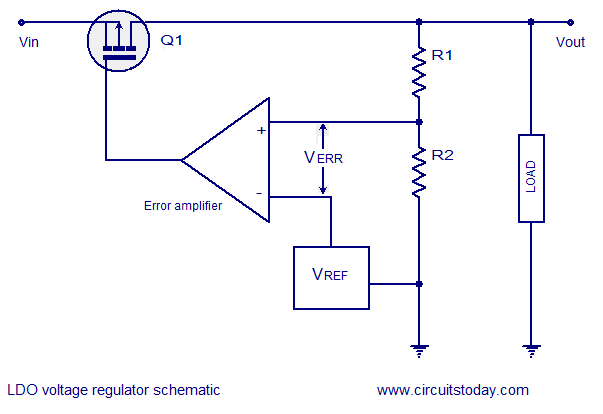
The image shown above is the schematic of a typical LDO voltage regulator. The working principle of LDO regulator is just like that of an ordinary linear voltage regulator. The essential components of an LDO voltage regulator are a reference voltage source, error amplifier and series pass element (BJT or MOSFET). The voltage drop across the series pass element is controlled by the error amplifiers output in order to control the output voltage. For example, suppose the load current decreases and as results the output voltage tends increase. This increase in output voltage will increase the error voltage (VERR).The output of the error amplifier will increase, making the series pass element ( P-Channel MOSFET) less conducting, which results in the reduction of the output voltage and the output voltage is brought back to the original level.
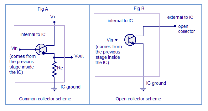
As I said above the working of a LDO voltage regulator is similar to the working of an ordinary linear voltage regulator and the only difference is in the schematic topology of their internal circuitry. Ordinary linear regulators (7805, LM117, LM317 etc) uses a common collector scheme while the LDO regulators use an open collector (termed as open drain if a MOSFET is used as the series pass element) scheme.
Common collector scheme.
Common collector scheme is one of the three basic transistor configurations. Here base is the input terminal, emitter is the output, and supply voltage is applied to the collector terminal. The series pass transistor inside an ordinary linear voltage regulator is wired in this configuration. Fig A shows the common collector scheme (also termed as emitter follower scheme).

Open collector scheme.
Many integrated circuits like LDO voltage regulators this scheme for wiring the series pass element (BJT or MOSFET). The input signal (which comes from the previous stage inside the IC) is coupled to the base of the BJT (or gate of the MOSFET), collector is left open and it is connected to a pin of the IC while the emitter is connected to the IC ground. This configuration makes it easy to saturate the series pass element and hence the dropout voltage is minimized.Fig B shows the open collector / drain scheme.
Practical LDO regulator circuit.

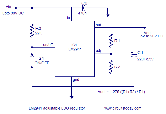
The circuit shown above is of a practical LDO regulator circuit using IC LM2941 from National semiconductors. LM2941 is an integrated LDO voltage regulator IC whose output can be adjusted. The IC has many good features like thermal shutdown, transient protection, short circuit protection etc. The reverse polarity protection feature makes this IC very applicable in automotive applications. The output voltage can be adjusted from 5V to 20V and the dropout voltage is 0.5V at 1A output current.
In the circuit the voltage divider network comprising of R1 and R2 sets the output voltage. Capacitor C2 is the input filter which is very essential if the regulator circuitry is situated away from the rectifier+filter module. Capacitor C1 is the output filter while S1 is the ON/OFF switch. Resistor R3 is used to ensure the necessary 300mA pull up current which is necessary for proper shutdown when the switch S1 is made open.
Notes.
- The circuit must be assembled on a good quality PCB.
- A heat sink is required for application above few hundred milli amps.
- Vout = 1.275 ((R1 + R2)/R1)
- During calculation select R1=1K and solve for R2.
- Selecting R1 = 1K will make the input bias current error of the adj pin negligible.
- Reducing the value of C1 below 22uF will induce instabilities and also this capacitor must be placed as close as possible to the IC on the PCB.

6 Comments
i want a practical variable output circuit using lm2951
nos besoins: limitation en courant , 3A
tension de sortie 24/30 V non régulée
drop out : 0.2 V max
quelle solution avec ou sans darlington ?
merci
I like this site. Because I always find something new to do. I want make a blog and I want your permission to upload all file to the blog. I won’t change or edit your file.