Introduction
The first step to digital signal processing is to convert a signal into digital data, and here the Analog to Digital Converter devices comes into action. Some of the AVR micro controllers include ADC unit in their features. This is a very useful unit for measurement related applications. The ADC used in AVR micro controllers are of successive approximation converter type. Read the Wikipedia article on SAR type ADC here. And you can read the Circuitstoday article too.
Using the ADC Unit
SAR type ADC needs these following things to run properly:
- A very stable, low internal impedance, very low noise DC Supply
- A Reference voltage
- A clock signal for the digital circuitry
And few input signals necessary for the control of operation these are
- ADEN, ADC Enable signal
- ADSC, ADC Start Conversion
- & Channel number to Multiplexer. This helps to select the ADC channel to perform a conversion operation.
Register Description & Minimum Configurations Required
|
ADC Multiplexer Selection Register – ADMUX |
||||||||
| Bit |
7 |
6 |
5 |
4 |
3 |
2 |
1 |
0 |
| Bit Name |
REFS1 |
REFS0 |
ADLAR |
– |
MUX3 |
MUX2 |
MUX1 |
MUX0 |
| Read/Write |
RW |
RW |
RW |
R |
RW |
RW |
RW |
RW |
| Initial value |
0 |
0 |
0 |
0 |
0 |
0 |
0 |
0 |
Bit 7:6 – REFS1:0: Reference Selection Bits
These bits select the voltage reference for the ADC, as shown in Table below. If these bits are changed during a conversion, the change will not go in effect until this conversion is complete (ADIF in ADCSRA is set). The internal voltage reference options may not be used if an external reference voltage is being applied to the AREF pin.
|
Interrupt Sense Control |
||
|
REFS1 |
REFS0 |
Voltage Reference Selection |
|
0 |
0 |
AREF, Internal VREF turned off |
|
0 |
1 |
AVcc with External capacitor at AREF pin |
|
1 |
0 |
Reserved |
|
1 |
1 |
Internal 2.56V Voltage Reference with external capacitor at AREF pin |
Bit 5 – ADLAR: ADC Left Adjust Result
Bits 3:0 – MUX3:0: Analog Channel Selection Bits
The value of these bits selects which analog inputs are connected to the ADC. See table below for details. If these bits are changed during a conversion, the change will not go in effect until this conversion is complete (ADIF in ADCSRA is set).
| Input Channel Selections | ||||
|
MUX3 |
MUX2 |
MUX1 |
MUX0 |
Selected ADC Channel |
|
0 |
0 |
0 |
0 |
ADC0 |
|
0 |
0 |
0 |
1 |
ADC1 |
|
0 |
0 |
1 |
0 |
ADC2 |
|
0 |
0 |
1 |
1 |
ADC3 |
|
0 |
1 |
0 |
0 |
ADC4 |
|
0 |
1 |
0 |
1 |
ADC5 |
|
0 |
1 |
1 |
0 |
ADC6 (Only for SMT Package) |
|
0 |
1 |
1 |
1 |
ADC7 (Only for SMT Package) |
|
1 |
0 |
0 |
0 |
|
|
1 |
0 |
0 |
1 |
|
|
1 |
0 |
1 |
0 |
|
|
1 |
0 |
1 |
1 |
|
|
1 |
1 |
0 |
0 |
|
|
1 |
1 |
0 |
1 |
|
|
1 |
1 |
1 |
0 |
1.30V (VBG) |
|
1 |
1 |
1 |
1 |
0V (GND) |
Bit 7 – ADEN: ADC Enable
Writing this bit to one enables the ADC. By writing it to zero, the ADC is turned off. Turning the ADC off while a conversion is in progress, will terminate this conversion.
Bit 6 – ADSC: ADC Start Conversion
In Single Conversion mode, write this bit to one to start each conversion. This first conversion performs initialization of the ADC. ADSC will read as one as long as a conversion is in progress. When the conversion is complete, it returns to zero. Writing zero to this bit has no effect.
Bit 5 – ADFR: ADC Free Running Select
Bit 4 – ADIF: ADC Interrupt Flag
This bit is set when an ADC conversion completes and the Data Registers are updated. The ADC Conversion Complete Interrupt is executed if the ADIE bit and the I-bit in SREG are set. ADIF is cleared by writing a logical one to the flag. Beware that if doing a Read-Modify- Write on ADCSRA, a pending interrupt can be disabled.
Bit 3 – ADIE: ADC Interrupt Enable
|
ADC Control and Status Register A – ADCSRA |
||||||||
| Bit |
7 |
6 |
5 |
4 |
3 |
2 |
1 |
0 |
| Bit Name | ADEN |
ADSC |
ADFR |
ADIF |
ADIE |
ADPS2 |
ADPS1 |
ADPS0 |
| Read/Write |
RW |
RW |
RW |
RW |
RW |
RW |
RW |
RW |
| Initial value |
0 |
0 |
0 |
0 |
0 |
0 |
0 |
0 |
Bits 2:0 – ADPS2:0: ADC Prescaler Select Bits
These bits determine the division factor between the XTAL frequency and the input clock to the ADC.
| ADC Prescaler Selections | |||
|
ADPS2 |
ADPS1 |
ADPS0 |
Division Factor |
|
0 |
0 |
0 |
2 |
|
0 |
0 |
1 |
2 |
|
0 |
1 |
0 |
4 |
|
0 |
1 |
1 |
8 |
|
1 |
0 |
0 |
16 |
|
1 |
0 |
1 |
32 |
|
1 |
1 |
0 |
64 |
|
1 |
1 |
1 |
128 |
The ADC Data Register – ADCL and ADCH
When an ADC conversion is complete, the result is found in these two registers. When ADCL is read, the ADC Data Register is not updated until ADCH is read. Consequently, if the result is left adjusted and no more than 8-bit precision is required, it is sufficient to read ADCH. Otherwise, ADCL must be read first, then ADCH. The ADLAR bit in ADMUX, and the MUXn bits in ADMUX affect the way the result is read from the registers. If ADLAR is set, the result is left adjusted. If ADLAR is cleared (default), the result is right adjusted
So to work with ADC, First of all, initial adjustments are necessary. And we need another function that initiates a conversion and generates a result. Let’s have look to the Codes:
void init() //Initiation Sequence

{ ADMUX |= (0<<REFS0)|(0<<REFS1); // Selecting the voltage reference

ADCSRA |= (1<<ADEN)|(1<<ADPS2)|(1<<ADPS1)|(1<<ADPS0); // Select Prescaler Frequency and Enable ADC

}
int doConversion(char Channel_Number) // ADC Read Operation Sequence
{ ADMUX = (Channel_Number&0x0f)|(ADMUX&0xf0); // Set up the Multiplexer to Read Desired Channel
ADCSRA |= (1<<ADSC); // Start the conversion sequence
while(!(ADCSRA&(1<<ADIF))); //Wait until the ADIF Flag goes High. ADIF Indicates conversion completion
return ADC; // Return result to calling function
}
Code
Textbox: Code for the Experiment
#define F_CPU 1000000

#include

#include

#include

void init()

{ ADMUX |= (0<<REFS0)|(0<<REFS1);

ADCSRA |= (1<<ADEN)|(1<<ADPS2)|(1<<ADPS1)|(1<<ADPS0);

}
int doConversion(char Channel_Number)
{ ADMUX = (Channel_Number&0x0f)|(ADMUX&0xf0);
ADCSRA |= (1<<ADSC);
while(!(ADCSRA&(1<<ADIF)));
return ADC;
}
int main()
{ initLCD();
init();
printf(“ADC Ch.1 Value=”);
LCDcmd(0xc0); while(1)
{ printf(” “);
LCDcmd(0xc0);
printf(“%d”,doConversion(0));
_delay_ms(700);
}
return 0;
}
Textbox: Code of ‘ATmega8LCDcfg1.h’
#ifdef _LCD_CFG_H

#warning "LCD configuration file already loaded. ATmega8LCDcfg.h inclusion skipped."

#endif

#ifndef _LCD_CFG_H

#define _LCD_CFG_H 1

#ifndef _AVR_IO_H_

#include

#endif

#ifndef _UTIL_DELAY_H_

#include

#endif

#ifndef _STDIO_H_

#include

#endif

#define DEL1 10

#define DEL2 40

#ifndef DPORT

#define DPORT PORTB

#endif

#ifndef CPORT

#define CPORT PORTD

#endif

#ifndef DPDDR

#define DPDDR DDRB

#endif

#ifndef CPDDR

#define CPDDR DDRD

#endif

#ifndef RS

#define RS PD6

#endif

#ifndef EN

#define EN PD7

#endif

int LCD(char ch, FILE *fp);

// Function To send a single char. to LCD

void LCDcmd(char ch);

void initLCD();

static  FILE lcd_str= FDEV_SETUP_STREAM(LCD,NULL,_FDEV_SETUP_WRITE);

/*

// Above: A stream is set up to give a formatted output

// to LCD using a macro FDEV_SETUP_STREAM(). The stream

// includes the function 'LCD()' that describes how a

// single character is sent to LCD. But the function

// prototype of 'LCD()' must be as per demand by the macro

// 'FDEV_SETUP_STREAM()'. See the prototype defined. This

// prototype is fixed. If this prototype difers. The program

// will not get complied.

// In the argument Field of 'FDEV_SETUP_STREAM(A,B,C)'. First

// field(A) holds the name of the function/routine that is to be

// used for sending a single charachter. Next field defines

// function to receive charachters. The next one defines if

// the stream to be set up can be used for reading charachters,

// writing charachters or both.

*/

void LCDcmd(char ch)

{ DPORT = ch;

CPORT = (1<<EN);

_delay_us(DEL1);

CPORT = (0<<EN);

_delay_us(DEL2);

if(ch==0x01||ch==0x02)

_delay_ms(10);

}

int LCD(char ch, FILE *fp)

{ DPORT =ch;

CPORT = (1<<EN)|(1<<RS);

_delay_us(DEL1);

CPORT = (0<<EN)|(0<<RS);

_delay_us(DEL2);

return 0;

}

void initLCD()

{ CPDDR = (1<<EN)|(1<<RS);

DPDDR = 0xff;

LCDcmd(0x38);

LCDcmd(0x0f);

LCDcmd(0x01);

LCDcmd(0x02);

stdout=&lcd_str;

}
Circuit Diagram
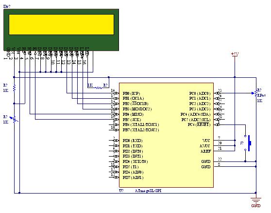
Picture: Circuit Diagram
3 Comments
Great article
Thanks for Publishing…
The only tutorial remaining is TWO Wire Interfacing! I hope someday I’ll come up with it!! 🙂 Now on!! There will be projects! good day!
Thank you, and good day,
Rakesh Bute
Jnior Author
Circuitstoday.com