Introduction
Micro controllers support wired communication protocols. Most of the time, microcontrollers come along with internal modules that support these protocols. The commonly supported protocols are:
- UART or USART communication
- SPI
- TWI
- USI etc.
And few advanced protocols like:
- USB
- CAN
- Ethernet etc.
SPI stands for Serial Peripheral Interface and it is the simplest among all the communication protocols. 8bit data registers in the devices are connected by wires. These data registers works as shift registers and one of the device controls the data exchange inside the SPI Network. The device or devices that controls the operation inside the network is known as the Master. For more elaboration, you may read the Wikipedia article: Serial Peripheral Interface Bus.
There can be multiple Masters in a system. There may be multiple slaves too. The slave need not to be another micro controller. It can be an SD card, or some display device or may be some other electronic circuit. Irrespective of the device attached as a slave, it needs to get selected by master device(s) for data transfer.
If the system is a multi-master network, then each individual secondary master needs to be selected for mastering the SPI BUS. An SPI bus consist of two DATA lines, one clock line, and device select (or slave select) lines. The clocking signal is generated by the master in the network.
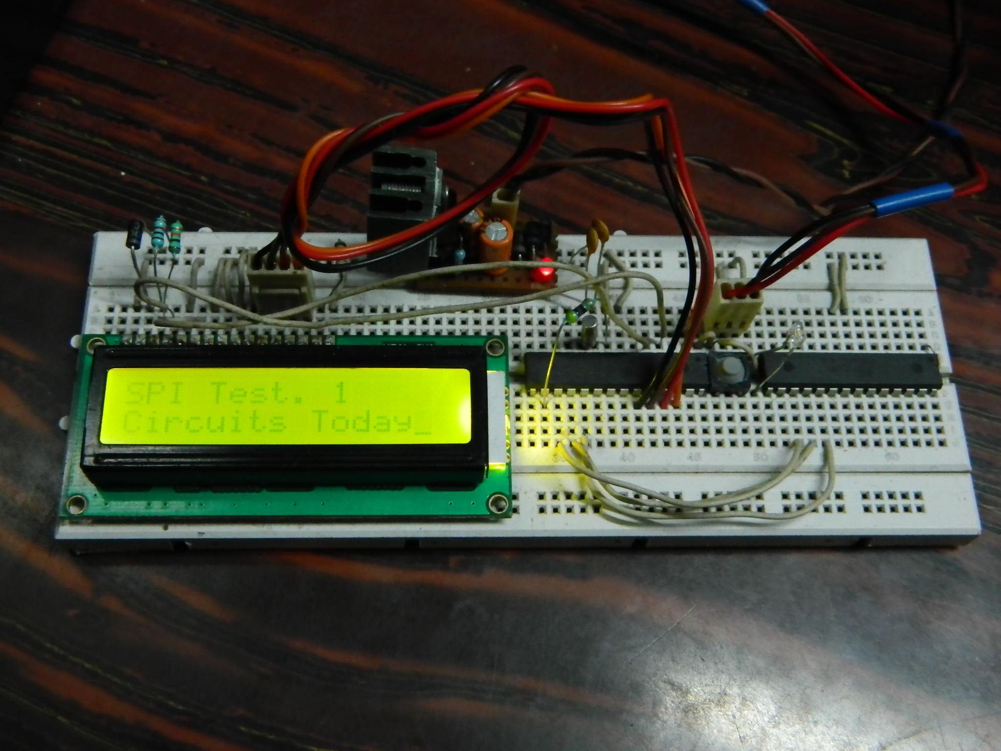
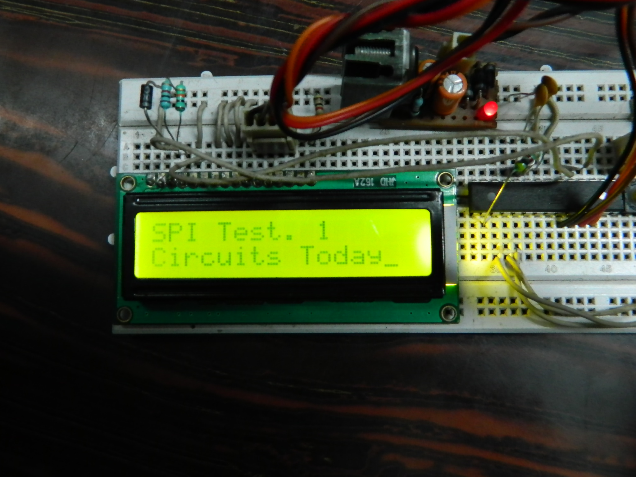
Here, in this experiment, one system is build up to receive any character transmitted in the SPI. And it displays the character on the LCD display. So the receiver circuit is essentially a slave. As the receiver system will never transmit any data, we can keep it enabled all the time. There would be a master device that will transmit a string of character, either once, or repetitively. So let’s see, what are the available resources for this communication.
Register Description
|
SPI Status Register- SPSR |
||||||||
| Bit |
7 |
6 |
5 |
4 |
3 |
2 |
1 |
0 |
| Bit Name |
SPIF |
WCOL |
– |
– |
– |
– |
– |
SPI2X |
| Read/Write |
R |
R |
R |
R |
R |
R |
R |
R |
| Initial value |
0 |
0 |
0 |
0 |
0 |
0 |
0 |
0 |
Bit 7 – SPIF: SPI Interrupt Flag
When a serial transfer is complete, the SPIF Flag is set. An interrupt is generated if SPIE in SPCR is set and global interrupts are enabled. If SS is an input and is driven low when the SPI is in Master mode, this will also set the SPIF Flag. SPIF is cleared by hardware when executing the corresponding interrupt Handling Vector. Alternatively, the SPIF bit is cleared by first reading the SPI Status Register with SPIF set, then accessing the SPI Data Register (SPDR).
Bit 6 – WCOL: Write Collision Flag
The WCOL bit is set if the SPI Data Register (SPDR) is written during a data transfer. The WCOL bit (and the SPIF bit) are cleared by first reading the SPI Status Register with WCOL set, and then accessing the SPI Data Register.
Bit 5..1 – Res: Reserved Bits
Bit 0 – SPI2X: Double SPI Speed Bit
When this bit is written logic one the SPI speed (SCK Frequency) will be doubled when the SPI is in Master mode . This means that the minimum SCK period will be 2 CPU clock periods. When the SPI is configured as Slave, the SPI is only guaranteed to work at or lower.
|
SPI Control Register- SPCR |
||||||||
| Bit |
7 |
6 |
5 |
4 |
3 |
2 |
1 |
0 |
| Bit Name |
SPIE |
SPE |
DORD |
MSTR |
CPOL |
CPHA |
SPR1 |
SPR0 |
| Read/Write |
RW |
RW |
RW |
RW |
RW |
RW |
RW |
RW |
| Initial value |
0 |
0 |
0 |
0 |
0 |
0 |
0 |
0 |
Bit 7 – SPIE: SPI Interrupt Enable
This bit causes the SPI interrupt to be executed if SPIF bit in the SPSR Register is set and the if the global interrupt enable bit in SREG is set.
Bit 6 – SPE: SPI Enable
When the SPE bit is written to one, the SPI is enabled. This bit must be set to enable any SPI operations.
Bit 5 – DORD: Data Order
Bit 4 – MSTR: Master/Slave Select
This bit selects Master SPI mode when written to one, and Slave SPI mode when written logic zero. If SS is configured as an input and is driven low while MSTR is set, MSTR will be cleared, and SPIF in SPSR will become set. The user will then have to set MSTR to re-enable SPI Master mode.
Bit 3 – CPOL: Clock Polarity
Bit 2 – CPHA: Clock Phase
Bits 1, 0 – SPR1, SPR0: SPI Clock Rate Select 1 and 0
These two bits control the SCK rate of the device configured as a Master. SPR1 and SPR0 have no effect on the Slave. The relationship between SCK and the Oscillator Clock frequency is shown in the following table:
|
Relationship Between SCK and the Oscillator Frequency |
|||
|
SPI2X |
SPR1 |
SPR0 |
SCK Frequency |
|
0 |
0 |
0 |
|
|
0 |
0 |
1 |
|
|
0 |
1 |
0 |
|
|
0 |
1 |
1 |
|
|
1 |
0 |
0 |
|
|
1 |
0 |
1 |
|
|
1 |
1 |
0 |
|
|
1 |
1 |
1 |
|
The SPI Data Register is a Read/Write Register used for data transfer between the Register File and the SPI Shift Register. Writing to the register initiates data transmission. Reading the register causes the Shift Register Receive buffer to be read.
|
SPI Data Register- SPCR |
||||||||
| Bit |
7 |
6 |
5 |
4 |
3 |
2 |
1 |
0 |
|
MSB |
LSB |
|||||||
| Read/Write |
RW |
RW |
RW |
RW |
RW |
RW |
RW |
RW |
| Initial value |
X |
X |
X |
X |
X |
X |
X |
X |
| X: Undefined | ||||||||
Points to be Noted.
- It is to be noted that when SPI is enabled, not all the pin function in the SPI ports are over ridden. Operations differ. Let’s have look on the effects.
|
Modes
|
Master |
Secondary master in Multi-Master mode |
Secondary master in Multi-Master mode |
Slave Mode |
|
Conditions |
The MSTR bit in SPCR is set (i.e. MSTR=1) |
The MSTR bit in SPCR is set (i.e. MSTR=1) |
The MSTR bit in SPCR is reset (i.e. MSTR=0) |
|
|
MOSI |
The relevant DDR bit must be set to 1 |
SPI overrides the pin functionality |
The relevant DDR bit must be set to 1 |
SPI overrides the pin functionality and configures the DDR bit to 0 |
|
MISO |
SPI overrides the pin functionality and configures the DDR bit to 0 |
The relevant DDR bit must be set to 1 |
The relevant DDR bit must be set to 1 |
The relevant DDR bit must be set to 1 |
|
SCK |
The relevant DDR bit must be set to 1 |
SPI over rides the pin functionality |
The relevant DDR bit must be set to 1 |
SPI overrides the pin functionality and configures the DDR bit to 0 |
|
(Slave select) |
The relevant DDR bit must be set to 1 |
SS is Configured as Input |
SS is Configured as Input |
SPI overrides the pin functionality and configures the DDR bit to 0. The clock generator unit is Stopped |
| DDR: Data Direction Register | ||||
- To Enable SPI operation these simple steps are sufficient
a. SET the SPE bit in SPCR register.
b. SET or RESET the MSTR bit in SPCR register
c. Configure the Data Direction Register (DDR) of the digital I/O port to which the SPI belongs to. Configure it as required
d. It’s not necessary to configure the Prescaler bits.
- SPI exchanges the contents of the SPDR of master and slave. So precautions should be taken so that garbage contents doesn’t get transmitted, or used.
Circuit Diagram
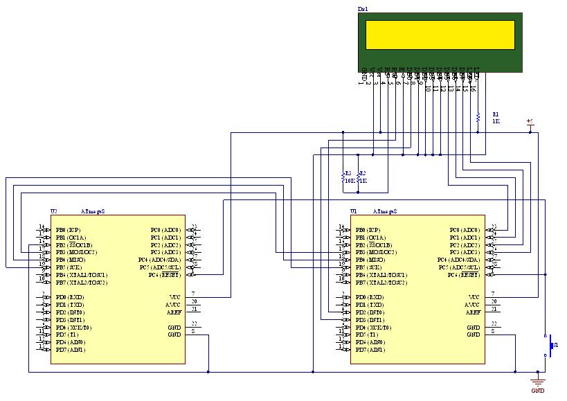
Refer this PDF file :- Working with SPI
Fig: Circuit Diagram
Codes
#ifndef _PROJECT_H
#define _PROJECT_H
#ifndef _AVR_IO_H_
#include<avr/io.h>
#endif
#ifndef _UTIL_DELAY_H_
#include<delay.h>
#endif
#ifndef _STDIO_H_
#include<stdio.h>
#endif
#ifndef DPDDR
#define DPDDR DDRC
#endif
#ifndef CPDDR
#define CPDDR DDRD
#endif
#ifndef CPORT
#define CPORT PORTD
#endif
#ifndef DPORT
#define DPORT PORTC
#endif
#ifndef RS
#define RS PD2
#endif
#ifndef EN
#define EN PD3
#endif
#define DEL1 10
#define DEL2 45
int LCD(char ch, FILE *fp);
int LCD(char ch,FILE *fp)
{
DPORT=(ch>>4)&0x0f;
CPORT=(1<
_delay_us(DEL1);
CPORT=(1<
_delay_us(DEL1);
DPORT=(ch&0x0f);
CPORT=(1<
_delay_us(DEL1);
CPORT=(14)&0x0f;
CPORT=(0<
_delay_us(DEL1);
CPORT=(0<
_delay_us(DEL1);
DPORT=(ch&0x0f);
CPORT=(0<
_delay_us(DEL1);
CPORT=(0<
_delay_us(DEL2);
_delay_us(DEL2);
if(ch==0x01||ch==0x02)
_delay_ms(5);
}
void initLCD()
{
DDRC =0x0f;
DDRD =(1<
LCDcmd(0x28);
LCDcmd(0x0f);
LCDcmd(0x01);
LCDcmd(0x02);
stdout =fdevopen(LCD,NULL);
}
#endif //_PROJECT_H
Text : Code of the header file ‘LCD83.h’
#include
#define F_CPU 1000000
Text : Code of the Receiver Micro-Controller (Configured as Slave)
Media
12 Comments
DDRB = (1<
??? complete compound expression…pls didn't understand…tnx in advance
The video was set to private, so I can’t watch, I am new on SPI interfaces, so I wanna know what it is about.
please provide me with full code for “How to Work With SPI in AVR Micro Controllers”
i will be grateful to you.
I can understand the pain to make all the details about AVR step by step.
I am so impressed to have the full tutorial available on AVR and it very perfectly desiged in order.
I always prefer to work with ATmega16 or ATmega32,
since all the programming(ISP) and powersupply lines fall in-line.
I will be happy to see “How to work with TWI in AVR” also, which is also an important communication faciility available with AVR.
It is very useful when two AVRs are to be communicated.
Thanks a lot.
Well,
Thanks for the appreciation.
thanks it was use full for me to learn. . .
Thanks for this article..
Please ..
I want simple SPI sample code In c…
thanks too much .
hi sir
i m doing a project on simple character transmit from one avr to another avr through spi….but i m getting some errors when tranmit the data…………..in this project the lcd is connected at port B and the MISO ,MOSI ,SS ,SCK pins are also at PORT B…..so its also not printing the data on lcd…….how can i do better spi interface between two avr
@ram,
first of all, whenever you plan to make a project you should first map the resources properly. In the avr section you can find my other articles using PORT C or PORT D when I’m usig the SPI. I would suggest you to avoid using the PORT B while interfacing both the LCD and the SPI. Cause LCD requires a parallel bus for interface most of the time. And whenever you use some peripherals of the micro controllers, the peripherals are previllaged over the port functionality. And the behaviour is is really tough to understand for a beginner. Try another port AND OTHER SET OF PINS I hope you’ll be able get enough help for yourself. If you face problems further, just visit the page again.
Please learn to use the English grammer correctly. There is nothing more annoying than to have to re-read the information over and over again to understand it.
grammer > grammar
We’ll keep it mind. Thank you.