Programming ARM MCUs – What is Different?
There are very, very few engineers or electronics enthusiasts who started programming with ARM microcontrollers right away. Most come to ARM looking for higher processing capabilities, with a background in simple 8-bit MCUs.
In the previous article on How to Setup and Install the Development Environment for ARM , it was shown how to set up the Keil ARM tools to be able to compile programs and generate output files. However, before you proceed to writing programs for an ARM microcontroller, it is important to know some differences between ARM and the AVR, 8051 or PIC that you might have programmed in the past.
There are some very basic, fundamental differences in how they treat data and transfer data internally. Knowing these differences simplifies the understanding of ARM hardware for those who have programmed 8-bit microcontrollers in the past.
Register Sizes
The first major difference you will notice is in the size of registers. On AVR or other 8-bit microcontrollers, the user accessible register size is almost always 8-bit. The registers that must contain 16-bit data are usually accessed as a “high byte” and a “low byte”. It requires two read accesses to read 16-bit data.
This is different in ARM. The ARM core is 32-bit capable and is most efficient when used in 32-bit mode. Therefore, almost all register addresses are 4 bytes in width (32-bit). For example, to enable all pins of AVR port D as output, you would write
DDRD = 0xFF; // Set all 8 pins as output
But on ARM, to make all pins of port 0 as output, you would write
IO0DIR = 0xFFFFFFFF; // Set all 32 pins as output
That being said, note that the port pin numbers may range from Pn.0 to Pn.31, as the I/O ports are also 32-bit wide. Of course, not all pins may be available externally – just like with 8-bit microcontrollers.
You may also be wondering – what if you want to switch one pin to high without affecting the rest? The typical process on an AVR would be:
- Take the contents of the output register
- Logical OR with binary pin data you want to SET (set to ‘1’)
- Logical AND with compliment of binary pin data you want to RESET (clear, or set to ‘0’)
- Write the result back to the output register.
This, in short is called the read-modify-write sequence and is time consuming because of so many steps. ARM addresses this problem by making it available in hardware. Instead of just a PORTn register to write the bit values of all pins, ARM microcontrollers offer mask registers such as IOnSET and IOnCLR. Writing a ‘1’ to any bit of the register clears or sets the bit and leaves other bits unaffected. This enables very fast I/O toggling and control (over 15MHz!).
System Structure
This section considers the LPC214x (NXP Semiconductors) to illustrate how sections are organized within the ARM7 microcontroller.
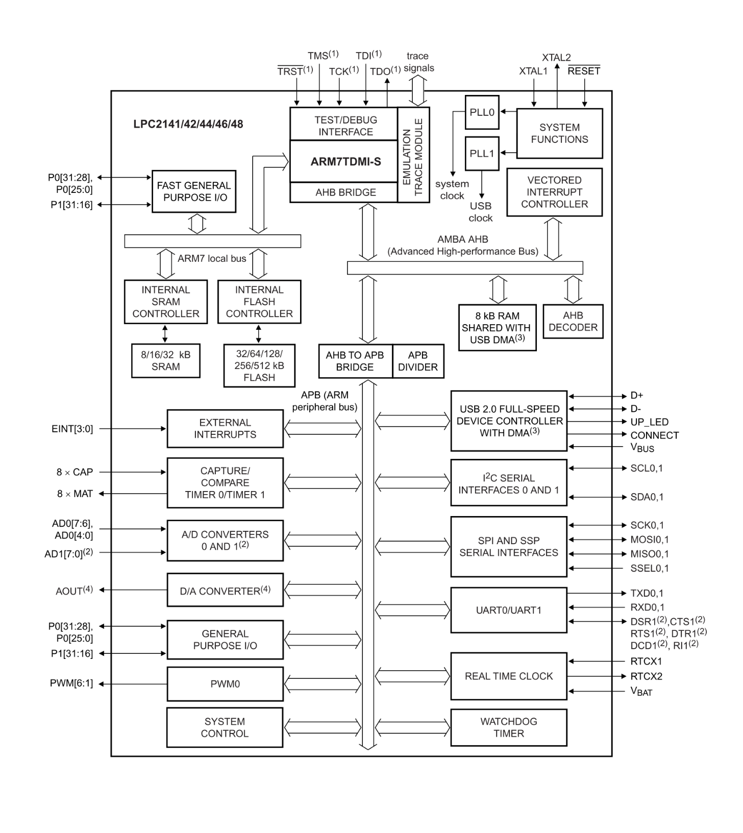
The central backbone network that can immediately be noticed is the VPB (VLSI Peripheral Bus). If you trace the bus upwards in the block diagram, you will notice that it originates from the AHB (Advanced High-performance Bus). The AHB runs at the same clock speed as the main ARM7TDMI-S core. The VPB obtains its clock from the AHB and the clock speed can be stepped down using a divider. The VPB connects all peripherals to the core. Therefore, the peripherals run at a speed lower or equal to the speed of the ARM core.
The interrupt controller and USB DMA (direct memory access) however run at the same speed as the core. This enables fast handling of interrupts and USB data transfers.
Knowing this structure makes the ARM microcontroller seem simpler to program, as each of these blocks are very easy to operate on. Also, knowing this structure is important to program applications without running into timing exceptions or errors (more on this below).
Timing
The ARM microcontroller integrates an ARM core and peripherals, as shown above. The peripherals are carefully integrated with the core. But the peripherals are also clearly separated in terms of clock source and speed. Therefore, it may be easy to cause timing issues without realizing what is happening. Debugging the program will rarely point this issue out.
To understand this, consider an example application which must detect a pulse of 0.3us (micro-second) or longer by using an external interrupt. Suppose that the external interrupt filter rejects pulses having width of less than 8 clock cycles as “glitches”. Thus, to detect a pulse of 0.3us, minimum clock speed is
8/(0.3us) = ~27MHz
For extra reliability, let us consider this as 30MHz.
So the conclusion is that you can set the CPU and interrupt controller speed to 30MHz to be able to detect this pulse using external interrupt. But this may NOT work!
Why? The external interrupt hardware is located on the VPB. Regardless of the processor frequency and the speed of VIC (interrupt controller), you need to step the VPB clock to 30MHz to detect this pulse. This is because the external interrupt hardware contains glitch filter that derives clock from the VPB clock, not the system clock.
Small issues like this may become very hard to debug, especially in case of high speed serial interfacing. A more detailed analysis will be included as we visit the peripherals individually in future articles.
Data Word Boundary Alignment
The register addresses MUST be accessed with word alignment. Half-word or byte access is not permitted. For example, you may read a word (32 bits) from a register located at 0x40000000 and 0x40000004. But you cannot write to the address 0x40000002.
This is because the address decoding logic in most chips do not implement byte lane hardware required for boundary independent access. The good thing is, this is not a big issue and it brings production costs down! The toolchain will take care of access rules for you when you program in C or other high level languages.
Also, the 32-bit address means that there is an address space of 4GB! Very few of these addresses are actually used and trying to access addresses that do not contain a register or memory will cause a bus cycle abort exception and will cause a reset if your code does not handle the exception properly. For this reason, it is highly recommended not to write ‘1’s to reserved bits or access unmapped addresses.
Typically, nothing would happen on most 8-bit MCUs when illegal accesses are made. An unrelated register may be affected or overwritten in the worst case. But on ARM MCUs, any illegal code behavior will cause exceptions. These must be handled by the user code.
In Keil tools, the exceptions just causes an infinite loop or reset by default – which is probably the safest way to handle an exception. This can be changed by modifying the assembly code in a startup file, which will be covered in more articles that follow.
1 Comment
If I am programming in a high-level language like C, why do I need to know details of internal structure/function like this? Is programming ARM fundamentally different that other MCUs, in that it’s more like assembly language, which requires so much hardware knowledge?