Half adder circuit.
To understand what is a half adder you need to know what is an adder first. Adder circuit is a combinational digital circuit that is used for adding two numbers. A typical adder circuit produces a sum bit (denoted by S) and a carry bit (denoted by C) as the output. Typically adders are realized for adding binary numbers but they can be also realized for adding other formats like BCD (binary coded decimal, XS-3 etc. Besides addition, adder circuits can be used for a lot of other applications in digital electronics like address decoding, table index calculation etc. Adder circuits are of two types: Half adder ad Full adder. Full adder s have been already explained in a previous article and in this topic I am giving stress to half adders.
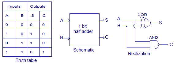
Half adder is a combinational arithmetic circuit that adds two numbers and produces a sum bit (S) and carry bit (C) as the output. If A and B are the input bits, then sum bit (S) is the X-OR of A and B and the carry bit (C) will be the AND of A and B. From this it is clear that a half adder circuit can be easily constructed using one X-OR gate and one AND gate. Half adder is the simplest of all adder circuit, but it has a major disadvantage. The half adder can add only two input bits (A and B) and has nothing to do with the carry if there is any in the input. So if the input to a half adder have a carry, then it will be neglected it and adds only the A and B bits. That means the binary addition process is not complete and that’s why it is called a half adder. The truth table, schematic representation and XOR//AND realization of a half adder are shown in the figure below.

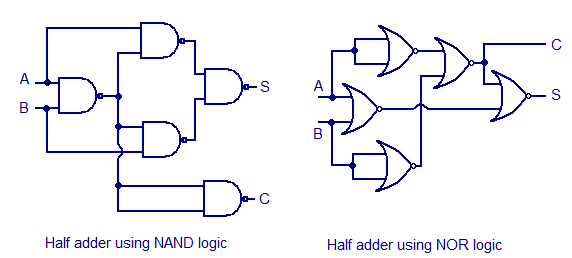
NAND gates or NOR gates can be used for realizing the half adder in universal logic and the relevant circuit diagrams are shown in the figure below.


20 Comments
I thnink this is among the so much significant information for me.
And i’m satisfied reading your article. But should commentary on few common things, The site style is wonderful, the articles is in point of fact nice : D.
Good task, cheers
selected question in BCA exam 2016
thank you….so much
can i have the logic diagram for half adder using nor gate only
useful information. thank u very much.
Excellent
FULL ADDER 3 IP 2OP
plz rply to my q as soon as possible???
why adder is called combinational ckt??
Bcoz combinational logic circuit is one which is solely depends upon the present state of the input. Not on the previous result. And even half adder also does not depend upon the previous results. I hope you’re clear now !!
Bcz it is combination of circuit like : And gate + exor gate like that perform half adder smiliary we can perform all arthmetic expersion using these gate using combining
A combinational circuit that performs the addition of the two binary numbers is called the half adder. … The operation is performed by the logic circuit called half adder. The half adder produces two binary digit as output, a sum bit and the carry bit and accepts two binary digit as input.
great ….. 🙂 work
oops sry!! its giving the right result
the half adder circuit with nor gates isnt giving the desired output
nice
Fine …..
half adder circuit
full adder circuit
nice…!!!