PLL Applications
1. Frequency Multiplication or Frequency Synthesis

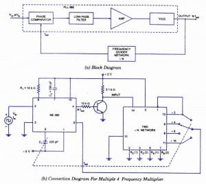
The block diagram of a frequency muliplier (or synthesizer) is shown in figure. In this circuit, a frequency divider is inserted between the output of the VCO and the phase comparator (PC) so that the loop signal to the PC is at frequency fOUT while the output of VCO is N fOUT. This output is a multiple of the input frequency as long as the loop is in lock. The desired amount of multiplication can be obtained by selecting a proper divide- by N network where N is an integer. Figure shows this function performed by a 7490 configured as a divide-by-4 circuit.
In this case the input Vin at frequency /in is compared with the output frequency fOUT at pin 5. An output at N fOUT (4 fOUT in this case) is connected through an inverter circuit to give an input at pin 14 of the 7490, which varies between 0 and + 5 V. Using the output at pin 9, which is one-fourth of that at the input to the 7490, the signal at pin 4 of the PLL is four times the input frequency as long as the loop remains in lock.
Since the VCO can be adjusted over a limited range from its centre frequency, it may become necessary to change the VCO frequency whenever the divider value is changed.
For verification of the circuit operation, one must determine the input frequency range and then adjust the free running fOUT of the VCO by means of R1 and C1 so that the output frequency of the 7490 divider is midway within the predetermined input frequency range. The output of VCO should now be equal to 4 fin.

5 Comments
the circuit provided is complecated.