Junction Characteristics
Before describing the fabrication sequences for ICs, it will be useful to provide insight into the use of epitaxial structures for devices.
A reverse-biased p-n junction can be considered to be a parallel-plate capacitor with the depletion region being the insulator or dielectric as shown in the figure below. The depletion or space-charge region is the region adjacent to the p-n junction that is essentially depleted (or devoid) of all mobile charges (that is, free electrons and holes), so that it acts like an insulator. For almost all diffused p-n junctions the doping on the diffused layer side of the junction will be very much heavier than the doping on the other (substrate) side of the junction, so that most diffused junctions can be considered to be one-sided junctions. The figure (a) corresponds to a general case of p-n junction, while figure (b) corresponds to a one-sided p-n junction. Notice that in the latter case the depletion region is almost entirely on the lightly doped (substrate) side of the junction and extends very little into the diffused layer side.
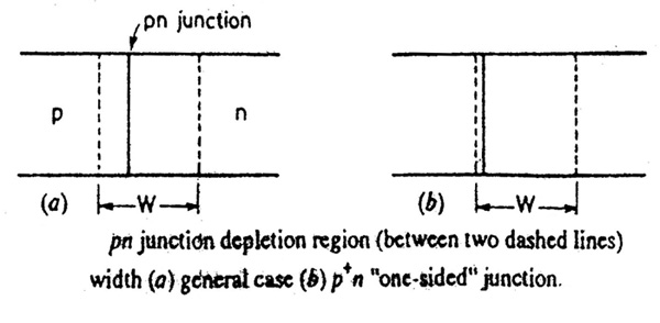
- P-N Junction Depletion Region
For a one sided junction, the breakdown voltage will be a function principal of the doping level on the more lightly doped side of the junction. The equation is given by
VZ = 2.7 * 1012 V/N2/3
The breakdown voltage for planar junctions will be somewhat lower than the values obtained from the above equation, especially at the lighter doping levels, where the breakdown voltage can be very substantially less, this is due to the effect of the junction curvature in the region underneath the edges of the oxide window, which results in an increase in the electric field intensity. At heavier doings, however, the influence of junction curvature on breakdown voltage becomes less. Therefore, for a high breakdown voltage a light doping is required. The junction depth should also not be too small especially for the cases in which very high breakdown voltages, typically more than 100 V, are required.
The bulk series resistance of a p-n junction is due to the finite resistivity of the p-type and n-type regions of the junction, outside the depletion region. For a p-n diffused junction the series resistance due to the p diffused layer will be negligible compared to the resistance due to the n-layer of the junction. Thus for a small value of series resistance a low-resistivity substrate is needed.
Epitaxial Structures
From the above discussion, we can consider the following requirements :
- For low junction capacitance Cj, low doping, that is, lightly doped substrate, is required.
- For high breakdown voltage, low doping, that is, lightly doped substrate, is required.
- For low series resistance, Rs, heavy doping, that is, low resistivity substrate is required.
We see that the series resistance requirement is conflicting with the capacitance and breakdown voltage requirements. The epitaxial structure shown in the figure below, offers a good way of resolving this conflict and simultaneously satisfying the capacitance, breakdown voltage and series resistance requirements. As long as the depletion region remains entirely within the lightly doped epitaxial layer and does not reach the heavily doped n+ substrate, the capacitance and breakdown voltage will be a function only of the epitaxial layer doping and will be independent of the substrate doping.
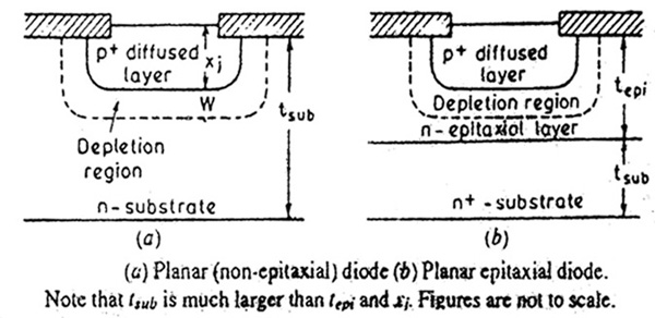
- Planar Epitaxial and Non-Epitaxial Diode
Planar Epitaxial Diode Fabrication Steps
After realizing the purpose of epitaxial layer, we will now summarize the processing steps tor some typical devices, starting with a planar p+n/n+ diode. Referring to figure (b) given above, the fabrication steps for the epitaxial planar diode are as follows.
- The starting material is n/n+ epitaxial wafer with a 0.005-ohm-cm (Sb-doped} substrate and an epitaxial layer of anywhere from 5 to 25 micro meters thick and phosphorus doped to resistivities in the range 5 to 50-ohm-cm.
- An oxide layer about 5000 to 8000A thick is grown.
- Using first photolithography windows are opened in the oxide layer for the P+ diffusion.
- A p+ diffused layer about 1 to 3 micro meters thick is produced to be the anode region of the diode.
- Using second photolithography anode contact windows are produced.
- Anode contacts are produced using aluminium deposition carried out by metallization process
- Using third photolithography the metallization is patterned for anode contacts.
- The metallization film is sintered or alloyed to form a good mechanical bond to the silicon and to produce a low- resistance, non rectifying ohmic contact. Sintering or alloying is a heat treatment at about 500 to 600°C.
- A back-side metallization is carried out. In this, a thin film of gold is evaporated on to the lapped back side of the wafers. This is for the eutectic die (chip) bonding of the chips to gold-plated headers or substrates at temperatures in the range 400° to 420°C, the gold/silicon eutectic temperature being 370°C.
Planar Epitaxial Transistor
The figure below shows a cross-sectional view of a typical n-p-n planar epitaxial transistor.
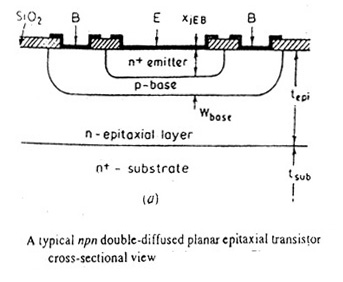
- Planar Epitaxial Transistor
The processing steps are as follows:
- The starting material is n/n+ epitaxial wafer with 0.005 ohm-cm Sb-doped substrate and n-type epitaxial layer of about 6 to 12 micro meters thickness and 0.3 to 3 ohm-cm resistivity.
- An oxide layer of about 5000 to 8000A thickness is grown.
- Using first photolithography, oxide windows arc etched for the base diffusion.
- A two-step deposition-drive in boron diffusion is performed for base region. The junction depth is about 2 to 3 micro meters. Sheet resistance is of about 200 ohm per square. The drive-in diffusion is performed in an oxidizing ambient so that oxide is regrown in the windows that were produced in the preceding step.
- Using second photolithography, oxide windows are etched for the emitter diffusion.
- A high surface concentration phosphorus diffusion is performed to produce an n+ diffused layer emitter region with a junction depth of about 2 to 2.5 micro meters.
- Using third photolithography, oxide windows are etched for emitter and base contacts.
- An aluminium thin film of about 0.5 to 1 micro meter separate thickness is deposited on the front surface of the surface using metallization process.
- Using fourth photolithography, windows are etched for emitter and base contact areas.
- Heat treatment at 500 to 600°C for sintering or alloying the metallization film is carried out.
- A gold thin film is deposited on the back side of the wafers.
Triple Diffused Planar Transistor
Early planar transistors and ICs used only photolithography and diffusion steps in the fabrication process. However, all diffused planar devices had severe limitations compared with discrete devices. In a triple diffused transistor as shown in the figure below, the collector region is formed by an n-type diffusion into the p-type wafer.
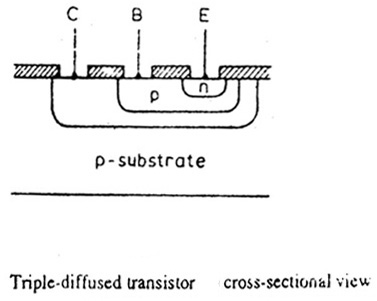
- Triple Diffused Transistor
The drawbacks of this structure are that the series collector resistance is high and the collector-to-emitter breakdown voltage is low. The former occurs because the impurity concentration in the portion of the collector diffusion below the collector-to-base junction is low giving the region high resistivity. The latter occurs because near the surface of the collector the concentration of impurities is relatively high, resulting in a low breakdown voltage between the collector and base diffusions. Thus the concentration profile provided by the diffused collector is very disadvantageous; what is required is a low impurity concentration at the collector-base junction for high breakdown voltage and a high concentration below the junction for low collector resistance. Such a concentration profile cannot be realized with diffusion alone, and hence the epitaxial growth was adopted. Epitaxial layer is thus a suitable starting material for the fabrication of bipolar transistors.
n-Channel JEET Fabrication Steps
The figure blow shows an n-channel epitaxial JEET structure. The n-type channel is formed by the n-type epitaxial layer region between the p+ diffused layer (gate) and the p-type substrate.
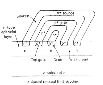
- n-Channel JFET Structure
The processing sequence for the device follows closely to that of the double-diffused transistor and is summarized below.
- The starting material is n/p epitaxial wafer.
- Thermal oxidation is carried out
- Using first photolithography, windows are opened for p+ boron top gate diffusion.
- Boron diffusion for gate region is carried out.
- Using second photolithography windows are opened for n+ source and drain diffusion.
- n+ phosphorus diffusion is carried out to produce the source and drain regions of the JFET. Using third photolithography, contact windows are opened
- Metallization is carried out.
- Using fourth photolithography metallization patterning for source, drain, and gale contact areas is carried out
- Contact sintering or alloying is done.
- Back-side metallization is carried out.

Comments are closed.