Double-Diffused MOS (DMOS)
In this article, the Double-Diffused MOS (DMOS) structure is explained with a diagram. The working of Vertical DMOS Transistor is also explained in detail with its structural analysis and diagram.
To know the basics of DMOS take a look at the following posts.
TAKE A LOOK : SHORT CHANNEL MOS STRUCTURES
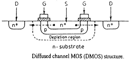
The figure below shows a double-diffused MOS (DMOS) structure. The channel length, L, is controlled by the junction depth produced by the n+ and p-type diffusions underneath the gate oxide. L is also the lateral distance between the n+ p junction and the p-n substrate junction. The channel length can be made to a smaller distance of about 0.5 micro meters. Thus, this process is similar to the situation with respect to the base width of a double-diffused bipolar transistor. When a fairly large positive voltage is applied to the gate [>VTH], it will cause the inversion of the p-substrate region underneath the gate to n- type , and the n-type surface inversion layer that is produced will act as a conducting channel for the flow of electrons from source to drain.
From the structure it is known that the n-type substrate is very lightly doped. This will help in making enough space for the expansion of the depletion region between the p-type diffusion region and the n+ drain contact region. Due to this, the breakdown voltage will become higher between the drain and source [BVDS].
Vertical DMOS Structure
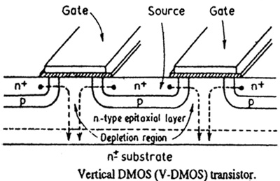
The figure below shows a vertical DMOS structure. In this case the drain contact region is the n+ substrate. If the n drain contact regions from the top surface is removed, more parallel-connected channels can be formed. This will naturally increase the transfer conductance and the drain current capability of the device. With a large high-density array of many gate electrodes on the top surface, vertical DMOS devices with current ratings of up to 10 A are possible.
The double-diffused MOS structure as shown above was one of the earlier successful efforts in the application of short-channel MOSFET technology. The name “DMOS” comes from the smanner of sequence in which the p- doped substrate is first diffused and later followed by highly doped n+ source diffusion. Further developments were made in the DMOS process so that it became one of major power FET technologies. But the first type of DMOS devices were very large in size due to their lateral structures. Because of this their advantages were soon offset. As a result vertical structures were designed and developed. There are two principal variations of vertical MOSFET structures. One variation is shown in the figure below. Another type of vertical MOS structure is discussed in the next post. To know more about it, click on the link below.
TAKE A LOOK : V-GROOVE MOS (VMOS)
As shon in the figure above, most of the high-voltage, high power DMOS structures are constructed with the source and gate located on the top of the chip-and the drain on the underside. VDMOS power FET’s have the power to withstand extremely high voltages with device ratings approaching the kilovolt range. Operationally, there is not much difference between the vertical structure and its planar or lateral equivalent. But VDMOS with smaller chip size have a higher yield. They also have a higher breakdown voltage.


2 Comments
abook cicuit radio puls tranmitter fm am