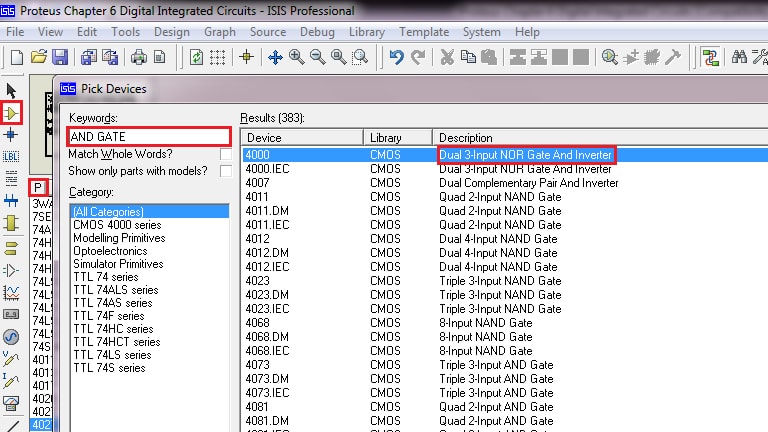
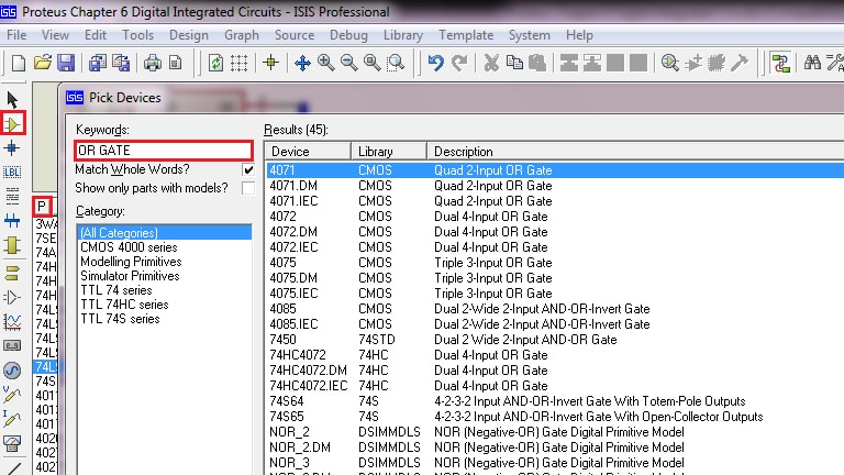
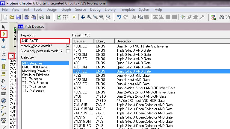
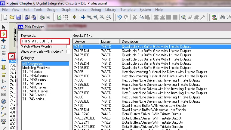
Proteus software has a big and vast collection of Digital IC library. This software can be used as an IC selector in digital circuits designing. Circuit designers don’t need to waste time searching the availability of various IC’s for the application. This library provides information of the IC’s along with their commercial nomenclatures and manufacturer details.
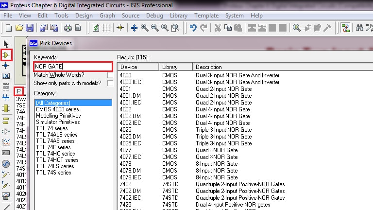
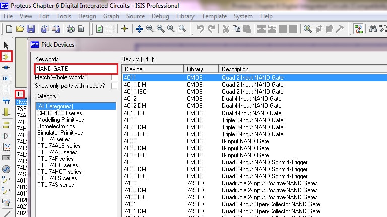
Components can be easily searched within the library using keywords like AND Gate, OR Gate, flip flops, decoders, counters etc. The description part provides information on the packages of the ICs, like the number of gates present in one IC etc. Preview is provided for ready reference of the component along with the PCB preview, and this makes it easy while converting the schematic model to PCB design.
Design techniques for proper simulation of digital circuits are mentioned below.
- Do not leave any of the input pins of IC’s open, i.e. on the floating state unless it is mentioned in the datasheet about internal pull-up up/pull down availability.
- Use resistors of suitable values, mostly 10K for external pull up or pull down.
- Using external pull up or pull down is must, while using manual switches as inputs.
- Use resistors of suitable values for LED loads. Do not connect LEDs directly to the outputs even for simulation purpose, as it may lead to incorrect operation of the circuit due to shifting of voltage levels.
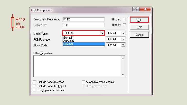
- It is advised to set model type of resistors in the resistor properties to Digital while using them with Digital ICs in the simulation software.
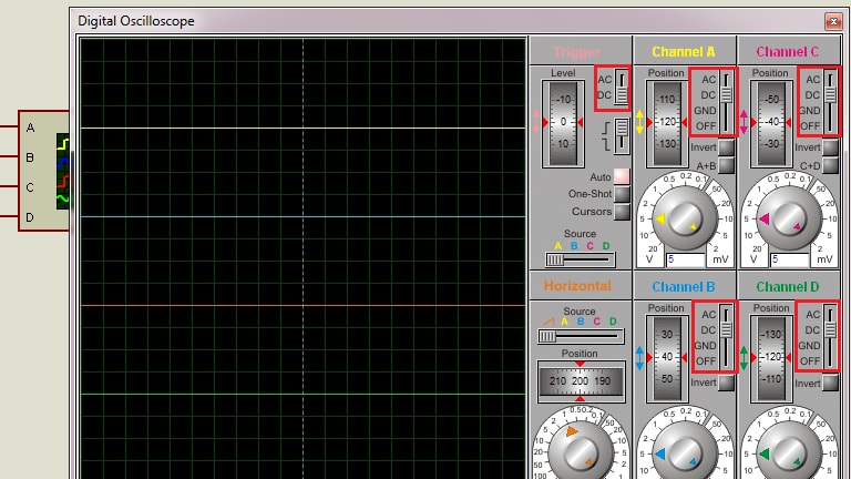
- While analyzing circuits with Oscilloscope, set the channels to DC mode.
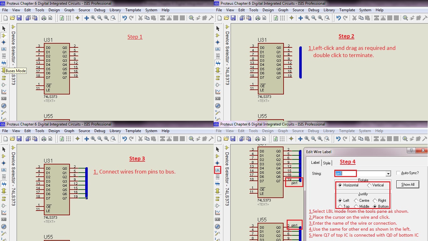
- Use Bus mode of wiring for connections if there are too many ICs or if the wiring is untidy.
- All the power pins like Vcc and GND of the ICs are internally connected and those pins are hidden.
- One can view the hidden pins of an IC in its properties tab. Right-click on the component and select edit properties.
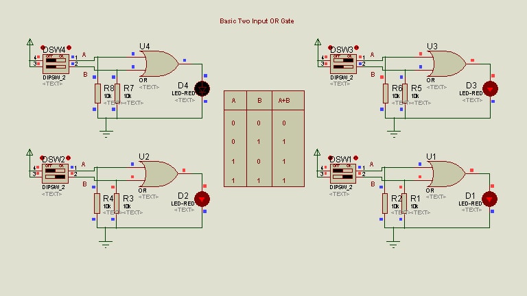
6.1 OR Gate
If any one of the inputs of OR Gate is HIGH, then the output of OR Gate is HIGH. If the inputs are applied manually using switches, the inputs must be pulled down for active high inputs and pulled up for active low inputs.
Truth Table of OR Gate
| A | B | A+B |
| 0 | 0 | 0 |
| 0 | 1 | 1 |
| 1 | 0 | 1 |
| 1 | 1 | 1 |
OR Gates with inputs up to 12 are available for simulation.However, for hardware implementation, the designer has to confirm their availability in the market from time-to-time
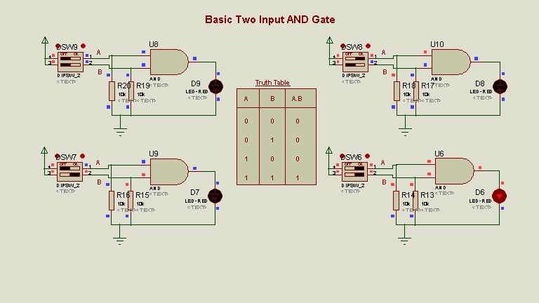
6.2 AND Gate
If all the inputs of AND Gate are HIGH, then the output of AND Gate is HIGH. If the inputs are applied manually using switches, the inputs must be pulled down for active high inputs and pulled up for active low inputs.
Truth Table of AND Gate
| A | B | A.B |
| 0 | 0 | 0 |
| 0 | 1 | 0 |
| 1 | 0 | 0 |
| 1 | 1 | 1 |
AND Gates with inputs up to 8 are available for simulation. However, for hardware implementation, the designers have to confirm their availability in the market from time-to-time
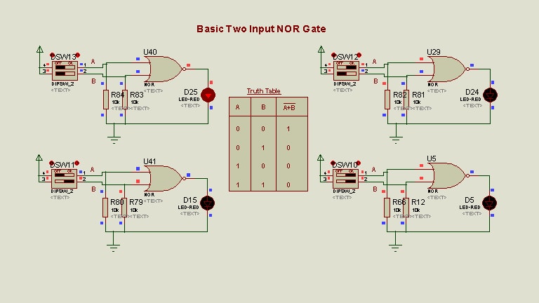
6.3 NOR Gate
If any one of the inputs of NOR Gate is HIGH then the output of NOR Gate is LOW. The output is HIGH only when all the inputs are LOW.
Truth Table of NOR Gate
| A | B | |
| 0 | 0 | 1 |
| 0 | 1 | 0 |
| 1 | 0 | 0 |
| 1 | 1 | 0 |
NOR Gate is one of the two universal gates i.e. any logic can be derived using NOR gates.NOR Gates with inputs up to 8 are available for simulation.
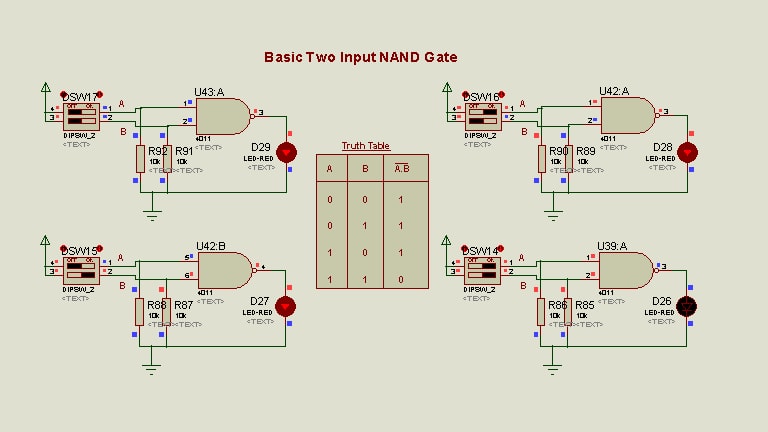
6.4 NAND Gate
If any one of the inputs of NAND Gate is LOW then the output of NAND Gate is HIGH. The output is LOW only when all the inputs are HIGH.
Truth Table of NAND Gate
| A | B | |
| 0 | 0 | 1 |
| 0 | 1 | 1 |
| 1 | 0 | 1 |
| 1 | 1 | 0 |
NAND Gate is one of the two universal gates i.e. any logic can be derived using NAND gates. NAND Gates with inputs up to 13 are available for simulation.
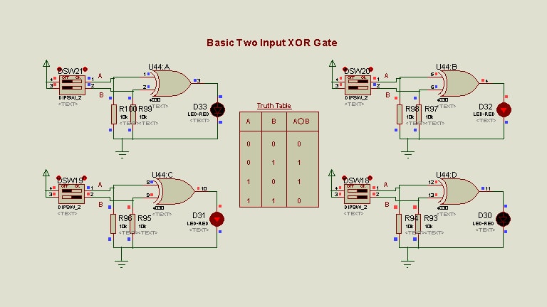
6.5 XOR Gate
If there is an Odd number of HIGH Inputs, then the output is HIGH. Two input X-OR gate function is similar to Two-Way switches in the electrical switchboards.
Truth Table ofXOR Gate
| A | B | AÅB |
| 0 | 0 | 0 |
| 0 | 1 | 1 |
| 1 | 0 | 1 |
| 1 | 1 | 0 |
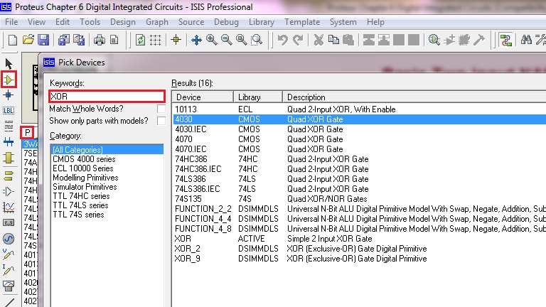
XOR Gate is a two bit Adder. XOR Gates with inputs up to 9 are available for simulation.
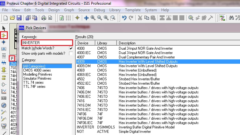
6.6 Inverter
The output of this gate is opposite to its input. It is a single input and single output gate.
Truth Table of Inverter
| A | Y= |
| 0 | 1 |
| 1 | 0 |
6.7 Buffer
The output of this gate is same as that of its input. It is a single input and single output gate. This is generally used to strengthen weak signal in any part of the circuit. Also, this is used to increase the propagation delay.
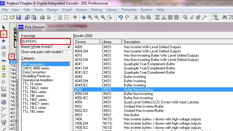
6.8 Buffers with Tri-state Output
The output of this gate is same as that of its input if the buffer is enabled. If the enable input is not active, then the output is in High impedance state or the Tri-state.
Outputs of two or more buffers can be connected together without the problem of short-circuiting. This property is useful in the input selection. IC packages with 6 Buffers are available.
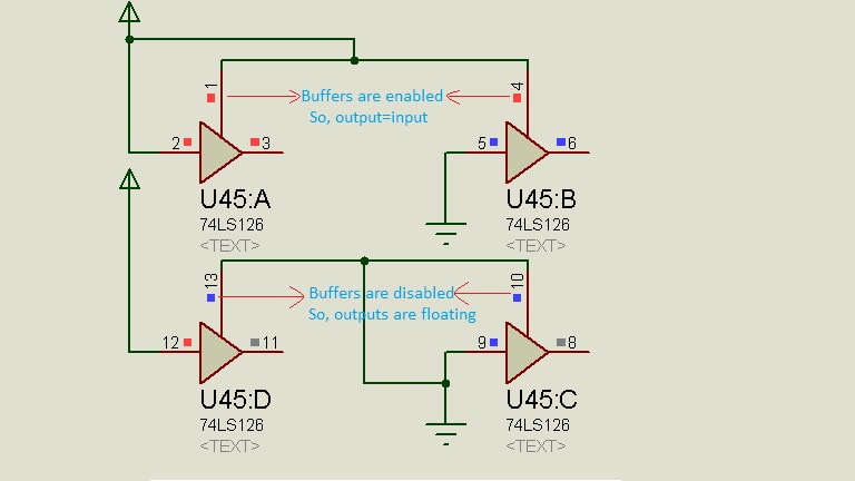
Data coming from one of the multiple channels can be selected using these buffers. This method can be employed to reduce the number of communication channels required in the processor, unless data from all the channels is required at a time.
6.9 Chip Selection / Stage Selection Technique
In large Digital circuits or multiple input/output systems, the central processor has to exchange data with its peripherals. The address lines of the processor contain the address of the particular peripheral. In order to enable the chip with a particular address, this chip selection technique is used.
This is achieved by using AND Gate with a suitable number of inputs as that of the address lines and some Inverters. For instance, let us not mind the source of address and consider three address lines through which addresses are obtained. So, AND Gate with 3 inputs is used. The number of possible addresses with 3-lines is 23=8.
With these 8 addresses, one of the 8 chips can be chosen. Each chip should be given a dedicated AND Gate, such that o/p of this gate is HIGH only when the address of the chip matches the address generated by address lines. This is typically called as 3 to 8 Decoder.
| Data Lines | I/Ps to AND Gate |
| D2D1D0 | I2I1I0 |
| 000 | 2 1 0 |
| 001 | 2 1 D0 |
| 010 | 2 D1 0 |
| 011 | 2D1 D0 |
| 100 | D2 1 0 |
| 101 | D2 1 D0 |
| 110 | D2 D1 0 |
| 111 | D2 D1 D0 |
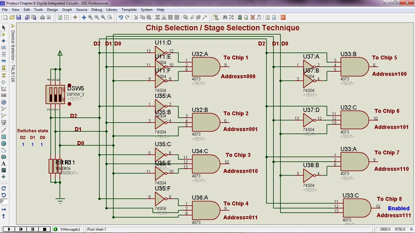
In the case of Binary counters, this technique is used for counter stage identification or selection to reset the counter or to start some other process. The number of chips addressed could be increased by increasing inputs of the AND Gate.
6.10 JK-Flip Flop
This is a two input Flip Flop whose output changes according to the inputs during the positive or negative edge of the clock signal. Hence, J and K are the synchronous inputs. They affect the output during the clock application.
State Transition of JK-Flip Flop
| J | K | Qn+1 |
| 0 | 0 | Qn |
| 0 | 1 | 0 |
| 1 | 0 | 1 |
| 1 | 1 | n |
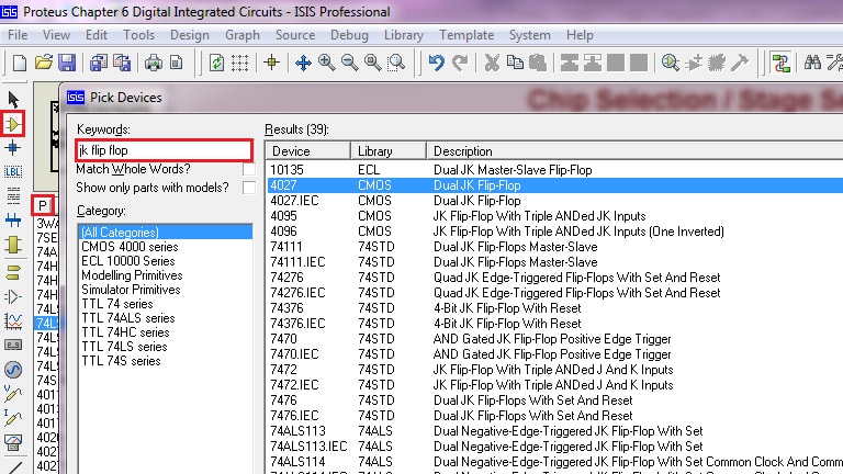
The clock for the Flip Flop can be selected i.e. Positive or Negative edge. Both are available. Asynchronous inputs are also included in the IC package, giving an option to Set/Reset the Flip Flop at any instant irrespective of the synchronous inputs and the clock signal. IC’s are fabricated with dual, triple, quadruple JK-Flip Flops in a single package with common as well as independent clock and asynchronous inputs.
JK Flip Flop operation
J=1,K=1 is the toggle state of the flip-flop, which leads to Toggle flip-flop i.e. output toggles continuously when positive clock edges are applied.
6.11 BCD Counter using JK-Flip Flops
JK Flip Flop is used as a base element in designing binary/BCD counters. Following is a 4-Bit Binary up-Counter. By cascading 4 JK Flip Flops, a 4-Bit counter is obtained.In both the counters the toggle state of the flip-flop i.e., with inputs J=K=1 is used.
If the output of one flip-flop is given as clock input to the next flip-flop, then up counter is obtained.
However, there are procedures for designing different counters, which are well explained in Digital electronics and switching circuit books.
6.12 D-Flip Flop
This is a Single input Flip Flop whose output changes according to the input during the positive or negative edge of the clock signal. This is also called as transparent Flip Flop.
State Transition of D-Flip Flop
| D | Qn+1 |
| 0 | 0 |
| 1 | 1 |
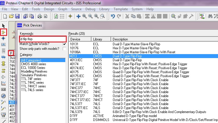
The clock for the Flip Flop can be selected i.e. Positive or Negative edge. Both are available. Asynchronous inputs are also included in the IC package, giving an option to Set/Reset the Flip Flop at any instant irrespective of the synchronous inputs and the clock signal. IC’s are fabricated with dual, triple, quadruple, hex, octal D Flip Flops in a Single package with output and input latch enable signal inputs. Hence, these flip-flops are used as latches.
D Flip Flop is used as a base element in designing Sequential circuits, counters, latches etc.Tri-state output option is also available in some IC’s like 74LS373. This allows Shunting of several similar ICs for selective data exchange, like extending PORTS of a microcontroller.
6.13 Decoders
Decoders are multi-input and multi-output combinational circuits. In case of address decoders only one of the outputs will be High at any instant. In the case of display decoders like the BCD to Seven segment decoders, the output will be according to the input data to lighten the desired segments of the display. Decoders with multiple enable inputs are called as De-Multiplexers.
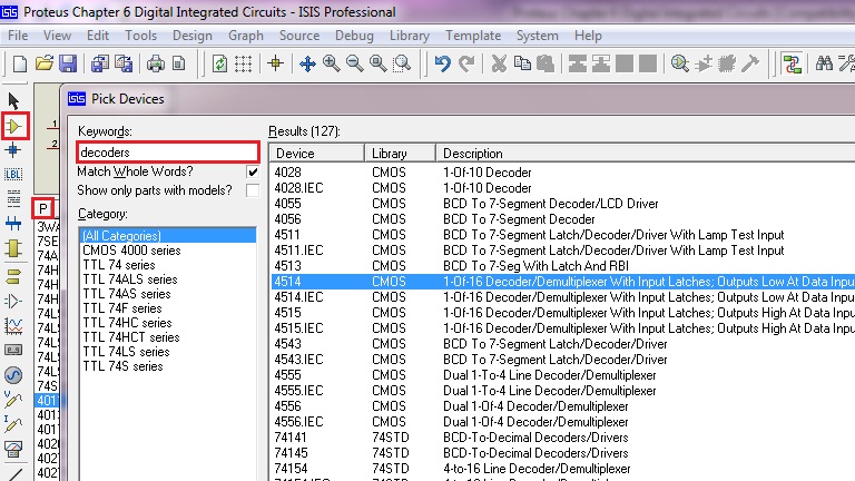
As in case of chip selection application, 4-Bit address is generated by a processor to the decoder. The decoder activates one of the outputs corresponding to the address at its inputs.
| PIN | Description | Logic |
| INH | Output Disable | High |
| STB | Output Latch Enable | High |
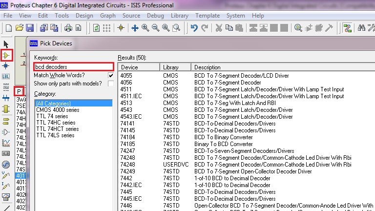
6.14 BCD to Seven segment decoder
BCD to Seven segment decoder is used to display BCD Values in decimal form. As in the binary counter example discussed above under JK-Flip Flop, the output is in binary form. By using this decoder, the count value can be displayed in decimal form.
| PIN | Description | Logic |
| LT | Lamp Test, to test the segments | Active Low |
| RBI=Ripple Banking Output | To avoid showing leading zeroes | Active low |
| RBO=Ripple Banking Input | Turns off the digit, used in brightness controlling by PWM | Active Low |
There are decoders for common cathode as well as common anode displays. Fonts are also different from one IC to other.
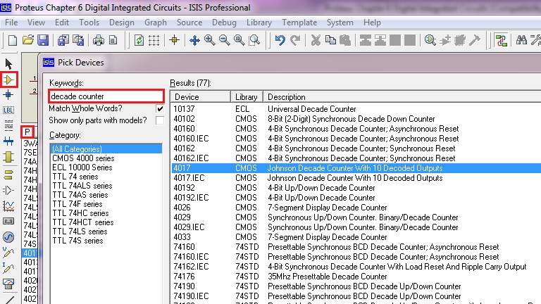
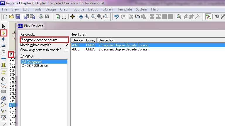
6.15 Decade counter
This is also one kind of decoder, which counts the input clock pulses and one of the ten outputs is made high corresponding to the counted incoming pulses.
| PIN | Description | Logic |
| CLK | Clock input | Positive edge |
| E | Clock enable input | Active low |
| CO | Carry Out, used as clock for succeeding counters,
divided by 10 counter |
Toggles after Q4 and Q9 |
| MR | Master Reset to reset the counter | Active High |
6.16 Pulse counter with seven segment output
This counter is a combination of binary counter, binary to BCD Converter, BCD to seven segment decoder. It has carry out and Un-gated C-segment outputs, which are used in Divided by 10 and Divided by 12 counters. These outputs are available even if display is disabled in power saving mode.
| PIN | Description | Logic |
| CLK | Clock input | Positive edge |
| DEI | Display enable input | Active High |
| INH | Inhibit input | High to stop counting |
| CO | Carry Out, used as clock for succeeding counters, divided by 10 counter | Become low for one clock period after every 10 cycles |
| MR | Master Reset to reset the counter | Active High |
| UCS | Un-gated C Segment output.
Used for divided by 12 counters. |
Same as C segment of the display, independent of DEI. |
| DEO | Display Enable Output | Same as DEI |
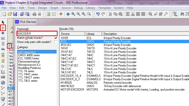
6.17 Priority Encoder
It is a multiple input multiple output IC, operates in reverse mode of 4 to 16 decoder.The output of the encoder is the binary value of the numerically highest active input. Hence, it is called as priority encoder. Consider a 16 to 4 Encoder with active high inputs. It has 16 inputs from D0 to D15 and 4-bit binary output. Under enabled state,
If D0=High, and all other inputs are low, then binary output = 0000.
If D15=High, irrespective of all other inputs, then binary output = 1111.
| PIN | Description | Logic |
| EI | Enable input | Active High |
| EO | Enable Output, used for cascading encoders | High only when all inputs are inactive |
| GS | Group Signal | High if at least one of the inputs is active, with EI=High. |
GS=Group Signal pin avoids the ambiguity of no active input state and D0 active state.
GS=High if at least one of the inputs is active. So, if output is binary 000 and GS=High, then it indicates that D0 is the active input.If output is binary 000 and GS=Low, then it indicates that no input is active. EO pin is used in cascading encoders for extending the overall encoder range.
Comments are closed.