To know about the different IC fabrication techniques, click on the link below.
TAKE A LOOK : IC FABRICATION TECHNIQUES
Diffusion of Dopant Impurities
The process of junction formation, that is transition from p to n type or vice versa, is typically accomplished by the process of diffusing the appropriate dopant impurities in a high temperature furnace. Impurity atoms are introduced onto the surface of a silicon wafer and diffuse into the lattice because of their tendency to move from regions of high to low concentration. Diffusion of impurity atoms into silicon crystal takes place only at elevated temperature, typically 900 to 1100°C.
Although these are rather high temperatures, they are still well below the melting point of silicon, which is at 1420°C. The rate at which the various impurities diffuse into silicon will be of the order of 1 micro meter per hour at a temperature range stated above, and the penetration depth that are involved in most diffusion processes will be of the order of 0.3 to 30 micro meter. At room temperature the diffusion process will be so extremely slow such that the impurities can be considered to be essentially frozen in place.
A method of p-n junction formation which was popular in the early days is the grown junction technique. In this method the dopant is abruptly changed in the melt during the process of crystal growth. A convenient technique for making p-n junction is the alloying of a metal containing doping atoms on a semiconductor with the opposite type of dopant. This is called the alloyed junction technique. The p-n junction using epitaxial growth is widely used in ICs. An epitaxial grown junction is a sharp junction. In terms of volume of production, the most common technique for forming p-n junctions is the impurity diffusion process. This produces diffused junction. Along with diffusion process the use of selective masking to control junction geometry, makes possible the wide variety of devices available in the form of IC’s. Selective diffusion is an important technique in its controllability, accuracy and versatility.
Nature of Impurity Diffusion
The diffusion of impurities into a solid is basically the same type of process as occurs when excess carriers are created non-uniformly in a semiconductor which cause carrier gradient. In each case, the diffusion is a result of random motion, and particles diffuse in the direction of decreasing concentration gradient The random motion of impurity atoms in a solid is, of course, rather limited unless the temperature is high. Thus diffusion of doping impurities into silicon is accomplished at high temperature as stated above.
There are mainly two types of physical mechanisms by which the impurities can diffuse into the lattice. They are
1. Substitutional Diffusion
At high temperature many atoms in the semiconductor move out of their lattice site, leaving vacancies into which impurity atoms can move. The impurities, thus, diffuse by this type of vacancy motion and occupy lattice position in the crystal after it is cooled. Thus, substitutional diffusion takes place by replacing the silicon atoms of parent crystal by impurity atom. In other words, impurity atoms diffuse by moving from a lattice site to a neighbouring one by substituting for a silicon atom which has vacated a usually occupied site as shown in the figure below.
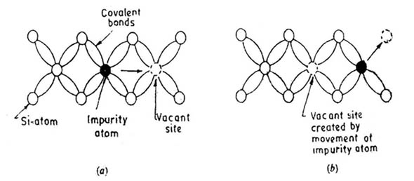
Substitutional diffusion mechanism is applicable to the most common diffusants, such as boron, phosphorus, and arsenic. These dopants atoms are too big to fit into the interstices or voids, so the only way they can enter the silicon crystal is to substitute for a Si atom.
In order for such an impurity atom to move to a neighbouring vacant site, it has to overcome energy barrier which is due to the breaking of covalent bonds. The probability of its having enough thermal energy to do this is proportional to an exponential function of temperature. Also, whether it is able to move is also dependent on the availability of a vacant neighbouring site and since an adjacent site is vacated by a Si atom due to thermal fluctuation of the lattice, the probability of such an event is again an exponent of temperature.
The jump rate of impurity atoms at ordinary temperatures is very slow, for example about 1 jump per 1050 years at room temperature! However, the diffusion rate can be speeded up by an increase in temperature. At a temperature of the order 1000 degree Celsius, substitutional diffusion of impurities is practically realized in sensible time scales.
2. Interstitial Diffusion
In such, diffusion type, the impurity atom does not replace the silicon atom, but instead moves into the interstitial voids in the lattice. The main types of impurities diffusing by such mechanism are Gold, copper, and nickel. Gold, particularly, is introduced into silicon to reduce carrier life time and hence useful to increase speed at digital IC’s.
Because of the large size of such metal atoms, they do not usually substitute in the silicon lattice. To understand interstitial diffusion, let us consider a unit cell of the diamond lattice of the silicon which has five interstitial voids. Each of the voids is big enough to contain an impurity atom. An impurity atom located in one such void can move to a neighbouring void, as shown in the figure below.
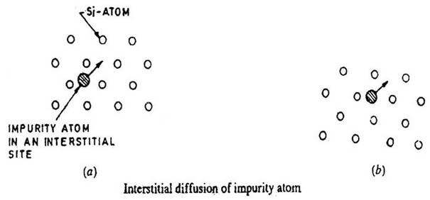
In doing so it again has to surmount a potential barrier due to the lattice, this time, most neighbouring interstitial sites are vacant so the frequency of movement is reduced. Again, the diffusion rate due to this process is very slow at room temperature but becomes practically acceptable at normal operating temperature of around 1000 degree Celsius. It will be noticed that the diffusion rate due to interstitial movement is much greater than for substitutional movement. This is possible because interstitial diffusants can fit in the voids between silicon atoms. For example, lithium acts as a donor impurity in silicon, it is not normally used because it will still move around even at temperatures near room temperature, and thus will not be frozen in place. This is true of most other interstitial diffusions, so long-term device stability cannot be assured with this type of impurity.
Fick’s Laws of Diffusion
The diffusion rate of impurities into semiconductor lattice depends on the following
- Mechanism of diffusion
- Temperature
- Physical properties of impurity
- The properties of the lattice environment
- The concentration gradient of impurities
- The geometry of the parent semiconductor
The behaviour of diffusion particles is governed by Fick’s Law, which when solved for appropriate boundary conditions, gives rise to various dopant distributions, called profiles which are approximated during actual diffusion processes.
In 1855, Fick drew analogy between material transfer in a solution and heat transfer by conduction. Fick assumed that in a dilute liquid or gaseous solution, in the absence of convection, the transfer of solute atoms per unit area in a one-dimensional flow can be described by the following equation
F = -D ∂N(x,t)/∂x = -∂F(x,t)/∂x
where F is the rate of transfer of solute atoms per unit area of the diffusion flux density (atoms/cm2-sec). N is the concentration of solute atoms (number of atoms per unit volume/cm3), and x is the direction of solute flow. (Here N is assumed to be a function of x and t only), t is the diffusion time, and D is the diffusion constant (also referred to as diffusion coefficient or diffusivity) and has units of cm2/sec.
The above equation is called Fick’s First law of diffusion and states that the local rate of transfer (local diffusion rate) of solute per unit area per unit time is proportional to the concentration gradient of the solute, and defines the proportionality constant as the diffusion constant of the solute. The negative sign appears due to opposite direction of matter flow and concentration gradient. That is, the matter flows in the direction of decreasing solute concentration.
Fick’s first law is applicable to dopant impurities used in silicon. In general the dopant impurities are not charged, nor do they move in an electric field, so the usual drift mobility term (as applied to electrons and holes under the influence of electric field) associated with the above equation can be omitted. In this equation N is in general function of x, y, z and t.
The change of solute concentration with time must be the same as the local decrease of the diffusion flux, in the absence of a source or a sink. This follows from the law of conservation of matter. Therefore we can write down the following equation
∂N(x,t)/∂t = -∂F(x,t)/∂x
Substituting the above equation to ‘F’. We get
∂N(x,t)/∂t = ∂/∂x[D*∂N(x,t)/∂x]
When the concentration of the solute is low, the diffusion constant at a given temperature can be considered as a constant.
Thus the equation becomes,
∂N(x,t)/∂t = D[∂2N(x,t)/∂x2]
This is Ficks second law of distribution.
Diffusion Profiles
Depending on boundary equations the Ficks Law has two types of solutions. These solutions provide two types of impurity distribution namely constant source distribution following complimentary error function (erfc) and limited source distribution following Gaussian distribution function.
Constant Source (erfc) Distribution
In this impurity distribution, the impurity concentration at the semiconductor surface is maintained at a constant level throughout the diffusion cycle. That is,
N (o,t) = NS = Constant
The solution to the diffusion equation which is applicable in this situation is most easily obtained by first considering diffusion inside a material in which the initial concentration changes in same plane as x=0, from NS to 0. Thus the equation can be written as
N (o,t) = NS = Constant and N(x,t) = 0
Shown below is a graph of the complementary error function for a range of values of its argument. The change in concentration of impurities with time, as described by the equation is also shown in the figure below. The surface concentration is always held at NS, falling to some lower value away from the surface. If a sufficiently long time is allowed to elapse, it is possible for the entire slice to acquire a dopant level of NS per m3.
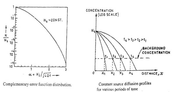
If the diffused impurity type is different from the resistivity type of the substrate material, a junction is formed at the points where the diffused impurity concentration is equal to the background concentration already present in the substrate.
In the fabrication of monolithic IC’s, constant source diffusion is commonly used for the isolation and the emitter diffusion because it maintains a high surface concentration by a continuous introduction of dopant.
There is an upper limit to the concentration of any impurity that can be accommodated at the semiconductor wafer at some temperature. This maximum concentration which determines the surface concentration in constant source diffusion is called the solid solubility of the impurity.
Limited Source Diffusion or Gaussian Diffusion
Here a predetermined amount of impurity is introduced into the crystal unlike constant source diffusion. The diffusion takes place in two steps.
1. Predeposition Step – In this step a fixed number of impurity atoms are deposited on the silicon wafer during s short time.
2. Drive-in step – Here the impurity source is turned off and the amounts of impurities already deposited during the first step are allowed to diffuse into silicon water.
The essential difference between the two types of diffusion techniques is that the surface concentration is held constant for error function diffusion. It decays with time for the Gaussian type owing to a fixed available doping concentration Q. For the case of modelling the depletion layer of a p-n junction, the erfc is modelled as a step junction and the Gaussian as a linear graded junction. In the case of the erfc, the surface concentration is constant, typically the maximum solute concentration at that temperature or solid solubility limit.
Parameters which affect diffusion profile
- Solid Solubility – In deciding which of the availability impurities can be used, it is essential to know if the number of atoms per unit volume required by the specific profile is less than the diffusant solid solubility.
- Diffusion temperature – Higher temperatures give more thermal energy and thus higher velocities, to the diffused impurities. It is found that the diffusion coefficient critically depends upon temperature. Therefore, the temperature profile of diffusion furnace must have higher tolerance of temperature variation over its entire area.
- Diffusion time – Increases of diffusion time, t, or diffusion coefficient D have similar effects on junction depth as can be seen from the equations of limited and constant source diffusions. For Gaussian distribution, the net concentration will decrease due to impurity compensation, and can approach zero with increasing diffusion tunes. For constant source diffusion, the net Impurity concentration on the diffused side of the p-n junction shows a steady increase with time.
- Surface cleanliness and defects in silicon crystal – The silicon surface must be prevented against contaminants during diffusion which may interfere seriously with the uniformity of the diffusion profile. The crystal defects such as dislocation or stacking faults may produce localized impurity concentration. This results in the degradation of junction characteristics. Hence silicon crystal must be highly perfect.
Basic Properties of the Diffusion Process
Following properties could be considered for designing and laying out ICs.
- When calculating the total effective diffusion time for given impurity profile, one must consider the effects of subsequent diffusion cycles.
- The erfc and Gaussian functions show that the diffusion profiles are functions of (x/ √Dt). Hence, for a given surface and background concentration, the junction depth x1 and x2 associated with the two separate diffusions having different times and temperature
- Lateral Diffusion Effects – The diffusions proceed sideways from a diffusion window as well as downward. In both types of distribution function, the side diffusion is about 75 to 80 per cent of the vertical diffusion.
Dopants and their Characteristics
The dopants selection affects IC characteristics. Boron and phosphorus are the basic dopants of most ICs. Arsenic and antimony, which are highly soluble in silicon and diffuse slowly, are used before epitaxial processing or as a second diffusion. Gold and silver diffuse rapidly. They act as recombination centres and thus reduce carrier life time.
Boron is almost an exclusive choice as an acceptor impurity in silicon since other p-type impurities have limitations as follows :
Gallium has relatively large diffusion coefficient in Si02, and the usual oxide window-opening technique for locating diffusion would be inoperative, Indium is of little interest because of its high acceptor level of 0.16 eV, compared with 0.01 eV for boron, which indicates that not all such acceptors would be ionized at room temperature to produce a hole. Aluminium reacts strongly with any oxygen that is present in the silicon lattice.
The choice of a particular n-type dopant is not so limited as for p-type materials. The n-type impurities, such as phosphorus, antimony and arsenic, can be used at different stages of IC processing. The diffusion constant of phosphorus is much greater than for Sb and As, being comparable to that for boron, which leads to economies resulting from shorter diffusion times.
Dopants in VLSI Technology
The common dopants in VLSI circuit fabrication are boron, phosphorus. and arsenic. Phosphorus is useful not only as an emitter and base dopant, but also far gettering fast-diffusing metallic contaminants, such as Cu and An, which cause junction leakage current problems. Thus, phosphorus is indispensable in VLSI technology. However, n-p-n transistors made with arsenic-diffused emitters have better low-current gain characteristics and better control of narrow base widths than those made with phosphorus-diffused emitters. Therefore, in V LSI, the use of phosphorus as an active dopant in small, shallow junctions and low-temperature processing will be limited to its use as the base dopant of p-n-p device and as a gettering agent. Arsenic is the most frequently used dopant for the source and drain regions in n-channel MOSFETs.
Diffusion Systems
Impurities are diffused from their compound sources as mentioned above. The method impurity delivery to wafer is determined by the nature of impurity source; Two-step diffusion is widely technique. Using this technique, the impurity concentration and profiles can be carefully controlled. The type of impurity distribution (erfc or Gaussian) is determined by the choice of operating conditions.
The two-step diffusion consists of a deposition step and a drive-in step. In the former step a constant source diffusion is carried out for a short time, usually at a relatively low temperatures, say, 1000°C. In the latter step, the impurity supply is shutoff and the existing dopant is allowed to diffuse into the body of the semiconductor, which is now held at a different temperature, say 1200°C, in an oxidizing atmosphere. The oxide layer which forms on tire surface of the wafer during this step prevents further impurities from entering, or those already deposited, from diffusing out. The final impurity profile is a function of diffusion condition, such as temperature, time, and diffusion coefficients, for each step.
- Diffusion Furnace
For the various types of diffusion (and also oxidation) processes a resistance-heated tube furnace is usually used. A tube furnace has a long (about 2 to 3 meters) hollow opening into which a quartz tube about 100,150 mm in diameter is placed as shown in the figure below.
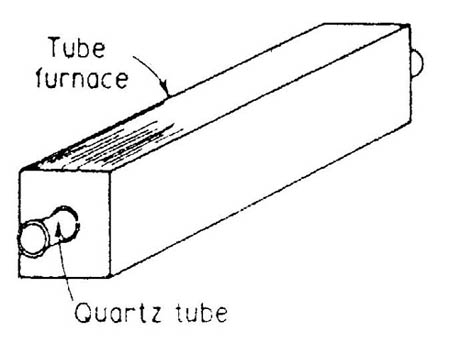
The temperature of the furnace is kept about1000°C. The temperature within the quartz furnace tube can be controlled very accurately such that a temperature within 1/2°C of the set-point temperature can be maintained uniformly over a “hot zone” about 1 m in length. This is achieved by three individually controlled adjacent resistance elements. The silicon wafers to be processed are stacked up vertically into slots in a quartz carrier or “boat” and inserted into the furnace lube.
Diffusion Of p-Type Impurity
Boron is an almost exclusive choice as an acceptor impurity in silicon. It has a moderate diffusion coefficient, typically of order I0-16 m2/sec at 1150°C which is convenient for precisely controlled diffusion. It has a solid solubility limit of around 5 x 1026 atoms/m3, so that surface concentration can be widely varied, but most reproducible results are obtained when the concentration is approximately 1024/m3, which is typical for transistor base diffusions.
- Boron Diffusion using B2H6 (Diborane) Source
This is a gaseous source for boron. This can be directly introduced into the diffusion furnace. A number of other gases are metered into the furnace. The principal gas flow in the furnace will be nitrogen (N2) which acts as a relatively inert gas and is used as a carrier gas to be a dilutent for the other more reactive gases. The N2, carrier gas will generally make up some 90 to 99 percent of the total gas flow. A small amount of oxygen and very small amount of a source of boron will make up the rest of the gas flow. This is shown in the figure below. The following reactions will be occurring simultaneously at the surface of the silicon wafers:
Si + 02 = SiO2 (silica glass)
2B2H6 + 302 = B2O3 (boron glass) + 6H2
This process is the chemical vapour deposition (CVD) of a glassy layer on (lie silicon surface which is a mixture of silica glass (Si02) and boron glass (B203) is called borosilica glass (BSG). The BSG glassy layer, shown in the figure below, is a viscous liquid at the diffusion temperatures and the boron atoms can move around relatively easily.
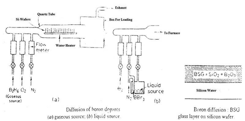
Furthermore, the boron concentration in the BSG is such that the silicon surface will be saturated with boron at the solid solubility limit throughout the time of the diffusion process as long as BSG remains present. This is constant source (erfc) diffusion. It is often called deposition diffusion. This diffusion step is referred as pre-deposition step in which the dopant atoms deposit into the surface regions (say 0.3 micro meters depth) of the silicon wafers. The BSG is preferable because it protects the silicon atoms from pitting or evaporating and acts as a “getter” for undesirable impurities in the silicon. It is etched off before next diffusion as discussed below.
The pre-deposition step, is followed by a second diffusion process in which the external dopant source (BSG) is removed such that no additional dopants cuter the silicon. During this diffusion process the dopants that are already in the silicon move further in and are thus redistributed. The junction depth increases, and at the same time the surface concentration decreases. This type of diffusion is called drive-in, or redistribution, or limited-source (Gaussian diffusion).
- Boron Diffusion using BBr3i (Boron Tribromide) Source
This is a liquid source of boron. In this case a controlled flow of carrier gas (N2,) is bubbled through boron tribromide, as shown in the figure below, which with oxygen again produces boron trioxide (BSG) at the surface of the wafers as per following reaction :
4BBr3 + 302 = B203 + 2Br2
Diffusion of n-Type Impurity
For phosphorus diffusion such compounds as PH3 (phosphine) and POCl3 (phosphorus oxychloride) can be used. In the case of a diffusion using PoCI3, the reactions occurring at the silicon wafer surfaces will be:
Si + 02 = SiO2 (silica glass)
4POCl + 302 = 2P205 + 6Cl2
This will result in the production of a glassy layer on the silicon wafers (hat is a mixture of phosphorus glass and silica glass called phosphorosilica glass (PSG), which is a viscous liquid at the diffusion temperatures. The mobility of the phosphorus atoms in this glassy layer and the phosphorus concentration is such that the phosphorus concentration at the silicon surface will be maintained at the solid solubility limit throughout the time of the diffusion process (similar processes occur with other dopants, such as the case of arsenic, in winch arsenosilica glass is formed on the silicon surface.
The rest of the process for phosphorus diffusion is similar to boron diffusion, that is, after deposition step, drive-in diffusion is carried out.
P205 is a solid source for phosphorus impurity and can be used in place of POCl3. However POCl3 offers certain advantages overP205 such as easier source handling, simple furnace requirements, similar glassware for low and high surface concentrations and better control of impurity density from wafer to wafer and from run to run.

4 Comments
Would you like to send me how to make an electric furnace or scheme, please?
sir explain acha kiya hua h
pls sent topics