We know that when the gate is biased negative with respect to the source in an N-channel JFET, the depletion region widths are increased. Theincrease in the depletion regions reduces the channel thickness, which increases its resistance. The net result is that drain current ID is reduced.
If the polarity of VGG were reversed so as to apply a positive bias to the gate with respect to source, the P-N junctions between the gate and the channel would then be forward biased. Since a forward bias reduces the width of a depletion region, the thickness of channel would increase with a corresponding decrease in channel resistance. As a result, drain current ID would increase beyond the JFET’s IDSS value.
The normal operation of a JFET is in its depletion mode of operation. However, as discussed above, it is also possible to enhance the conductivity of the JFET channel. However, the forward bias of the silicon P-N junction is usually restricted to a maximum of 0.5 V (more conservative limit is 0.2 V) so as to limit the gate current.
As we have seen that, the greater the ID is compared to IDSS the greater the transconductance gm will be. We have seen before that the voltage gain is directly proportional to gm. So, in general, the higher the gm, the better it is. This is one of the advantages of being able to enhance the channel.
As its name suggests, the depletion-enhancement MOSFET (DE-MOSFET)-was developed to be used in either or both the depletion and enhancement modes.
Construction of a DEMOSFET.

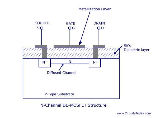
Figure shows the construction of an N-channel depletion MOSFET. It consists of a highly doped P-type substrate into which two blocks of heavily doped N-type material are diffused forming the source and drain. An N-channel is formed by diffusion between the source and drain. The type of impurity for the channel is the same as for the source and drain. Now a thin layer of SiO2 dielectric is grown over the entire surface and holes are cut through the SiO2 (silicon-dioxide) layer to make contact with the N-type blocks (Source and Drain). Metal is deposited through the holes to provide drain and source terminals, and on the surface area between drain and source, a metal plate isdeposited. This layer constitutes the gate. Si02 layer results in an extremely high input impedance of the order of 1010 to 1015 Q for this area. The chip area of a MOSFET is typically 0.003 um2 or less which is about only 5% of the area required by a BJT. A P-channel DE-MOSFET is constructed like an N-channel DE-MOSFET, starting with an N-type substrate and diffusing P-type drain and source blocks and connecting them internally by a P-doped channel region.
Operation of DEMOSFET.

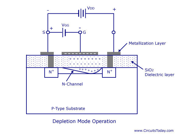
DE-MOSFET can be operated with either a positive or a negative gate. When gate is positive with respect to the source it operates in the enhancement—or E-mode and when the gate is negative with respect to the source, as illustrated in figure, it operates in depletion-mode.
When the drain is made positive with respect to source, a drain current will flow, even with zero gate potential and the MOSFET is said to be operating in E-mode. In this mode of operation gate attracts the negative charge carriers from the P-substrate to the N-channel and thus reduces the channel resistance and increases the drain-current. The more positive the gate is made, the more drain current flows.
On the other hand when the gate is made negative with respect to the substrate, the gate repels some of the negative charge carriers out of the N-channel. This creates a depletion region in the channel, as illustrated in figure, and, therefore, increases the channel resistance and reduces the drain current. The more negative the gate, the less the drain current. In this mode of operation the device is referred to as a depletion-mode MOSFET. Here too much negative gate voltage can pinch-off the channel. Thus operation is similar to that of JFET.
Characteristics of DEMOSFET.

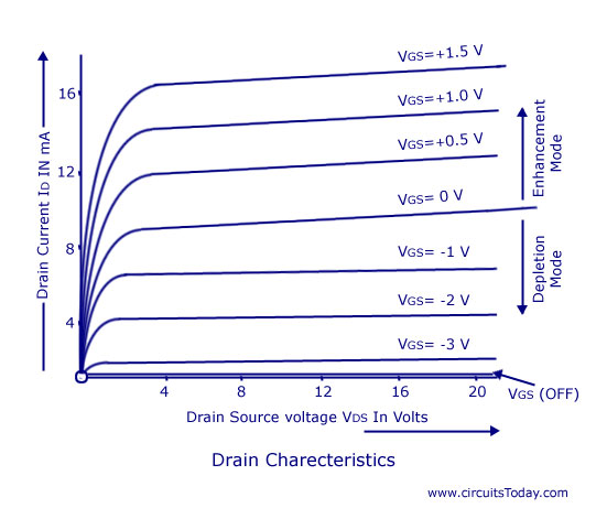
Typical drain characteristics, for various levels of gate-source voltage, of an N-channel MOSFET are shown in figure. The upper curves are for positive VGS and the lower curves are for negative VGS. The bottom drain curve is for VGS = V GS(OFF). For a specified drain-source voltage VDS, VGS (OFF) is the gate-source voltage at which drain current reduces to a certain specified negligibly small value, as shown in figure. This voltage corresponds to the pinch-off voltage Vp of JFET. For VGS between VGS (0FF) and zero, the device operates in depletion-mode while for VGS exceeding zero the device operates in enhancement mode. These drain curves again display an ohmic region, a constant-current source region and a cut-off region. MOSFET has two major applications: a constant current source and a voltage variable resistor.

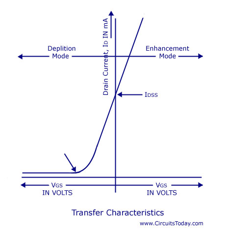
The transfer (or transconductance) characteristic for an N-channel DE-MOSFET is shown in figure. IDSS is the drain current with a shorted gate. Since the curve extends to the right of the origin, IDSS is no longer the maximum possibledrain current.
Mathematically, the curve is still part of a parabola and the same square-law relation exists as with a JFET. In fact, the depletion-mode MOSFET has a drain current given by the same transconductance equation as before, equation . Furthermore, it has the same equivalent circuits as a JFET. Because of this, the analysis of a depletion-mode MOSFET circuit is almost identical to that of a JFET circuit. The only difference is the analysis for a positive gate, but even here the same basic formulas are used to determine the drain current ID, gate-source voltage VGS etc.
The foregoing discussion is applicable in principle also to the P-channel DE-MOSFET. For such a device the sign of all currents and voltages in the characteristics must be reversed.
Schematic Symbols of DEMOSFET.

Figure shows the schematic symbol for a DE-MOSFET. Just to the right of the gate is the thin vertical line representing the channel. The drain lead comes out from the top of the channel and the source lead connects to the bottom. The arrow is on the P-substrate and points to the N-material. In some applications, a voltage can be applied to the substrate for added control of drain current. For this reason, some DE-MOSFETs have four terminal leads. But in most applications, the substrate is connected to the source. Usually the substrate is connected to the source internally by the manufacturer. This results in a three terminal device whose schematic symbol is shown in figure.
Schematic symbol for a three terminal P-channel DE-MOSFET device is shown in figure. The schematic symbol of a P-channel DE-MOSFET is similar to that of an N-channel DE-MOSFET, except that the arrow points outward.

5 Comments
it is a good website of electronics circuits and it is a good tropic of electronics.
one question that why we use silicon for mosfet?
why…with… increasing drain voltage……after sm time…current bcm constant? ????
We have DE MOSFET it works both in depletion mode and enhancement mode.then why we made another Enhancement mode only transistor?
lectures of MOSFET by IIT Madras professor
http://www.youtube.com/watch?v=g30xTHas3aU