In this article, we are explaining an astable multivibrator, often called a free-running multivibrator. An astable multivibrator can be designed using different types of components, say using transistors (and associated components) alone or by using op amps (and associated components). In this article, we are designing an Astable Multivibrator using 555 Timer IC.
If you are wondering what all are the practical applications of an astable multivibrator, lets begin by seeing a few. One of the most common application for an astable multivibrator is to generate time delays. Let’s say you want to turn an LED “ON” for 1 second and keep it “OFF” for 0.5 seconds, then an astable multivibrator is the best circuit you could use to build this application.
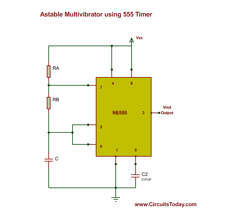
Unlike the monostable multivibrator, this circuit does not require any external trigger to change the state of the output, hence the name free-running. Before going to make the circuit, make sure your 555 IC is working. For that go through the article: How to test a 555 IC for working An astable multivibrator can be produced by adding resistors and a capacitor to the basic timer IC, as illustrated in figure. The timing during which the output is either high or low is determined by the externally connected two resistors and a capacitor. The details of the astable multivibrator circuit are given below.
So let’s begin to design an astable multivibrators using 555 timer IC. Let’s first draw the 555 timer astable multivibrator circuit.
555 Timer Astable Multivibrator Circuit Diagram
An Astable Multivibrator can be designed by adding two resistors (RA and RB in circuit diagram) and a capacitor (C in circuit diagram) to the 555 Timer IC. These two resistors and the capacitor (values) are selected appropriately so as to obtain the desired ‘ON’ and ‘OFF’ timings at the output terminal (pin 3). So basically, the ON and OFF time at the output (i.e the ‘HIGH’ and ‘LOW’ state at the output terminal) is dependent on the values chosen for RA,RB and C. We will see more about this on the astable multivibrator design section given below.
Note:- The capacitor C2 (0.01uF) is connected to pin number 5 (Control Voltage Terminal) in all 555 IC based circuits in which that particular pin (pin 5 – control voltage terminal)is not used. This capacitor is used to avoid noise problems that could arise in the circuit if that pin is left open.
Take a look @ 555 Ic Pin configuration and 555 block diagram before reading further.
The Connections
Let’s see how the 555 timer astable multivibrator connections are made in the circuit diagram.
Pin 1 is grounded; pins 4 and 8 are shorted and then tied to supply +Vcc, Output (Vout) is taken from pin 3; pin 2 and 6 are shorted and then connected to ground through the capacitor C to ground terminal, pin 7 is connected to supply + VCC through a resistor RA; and between pin 6 and 7 a resistor RB is connected. At pin 5 either a bypass capacitor (to bypass noise signals) of 0.01uF is connected or modulation input is applied.
Astable Multivibrator Working
So far we have seen how an astable multivibrator is designed using 555 timer IC, the circuit diagram and how the pin connections are made. Now let’s see the operation and working of an astable multivibrator. To explain the 555 timer astable multivibrator working, we have drawn an internal circuit diagram of 555 timer IC (consisting of two Op Amps, an SR Flip Flop and the transistor connected at the discharging terminal – pin 7) along with the necessary external connections (RA, RB and C). Wave forms from the output terminal (Vout – pin 3) is shown towards the right side of the circuit diagram. Carefully observe the circuit diagram and the output waveforms before we begin the explanation.

The basic objective of an astable multivibrator is to switch the output status (from HIGH to LOW and from LOW to HIGH) at the desired time intervals, without any external intervention (say an input trigger pulse like in the case of monostable multivibrator). We achieve this (in a 555 IC) by controlling the discharge terminal (pin 7) of 555 IC through a capacitor (C). Inside the 555 IC, this discharge terminal (pin 7) is connected to the collector terminal of a transistor whose base is directly connected to the output terminal (non inverting terminal – Q) of SR flip flop. You have to notice that Vout (pin 3 – output terminal of 555 IC) is taken from the inverting output terminal (Q complimentary terminal) of SR flip flop. So when when flip flop output (non inverting) Q is HIGH, Vout will be LOW and when flip flop output Q is LOW, Vout will be HIGH.
Now let’s see how the automatic switching of ON and OFF state at the Vout terminal is achieved by the capacitor C connected to the dicharge terminal -pin 7.
You may also recall the Block Diagram (given below) and the Working Principle of 555 IC, explained in our previous chapter/tutorial on 555 Timer.
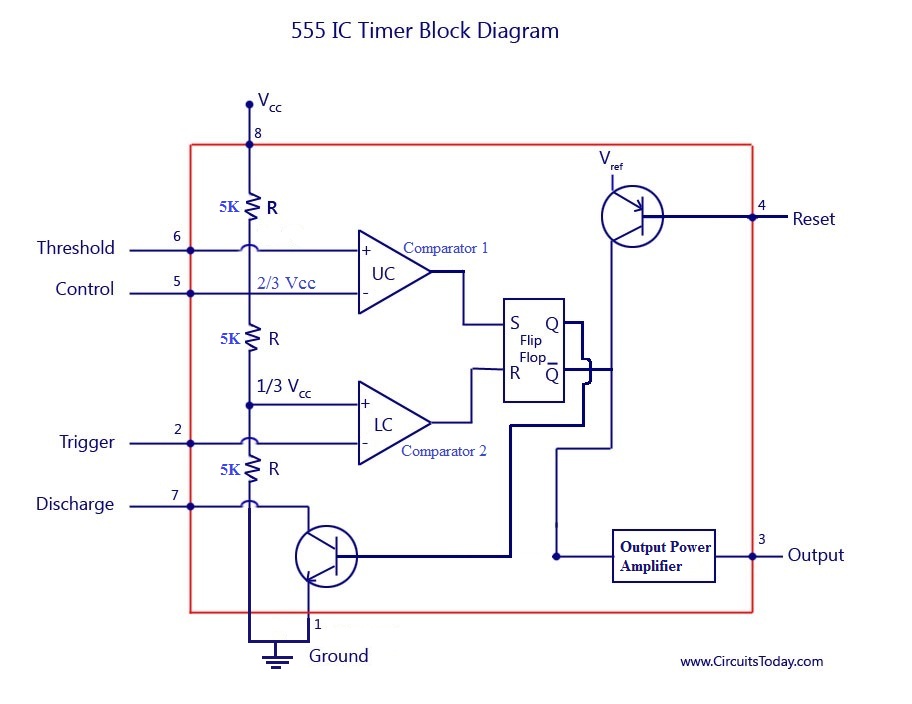
The block diagram of a 555 timer is shown in the above figure. A 555 timer has two comparators (which are basically 2 op-amps), an R-S flip-flop, two transistors and a resistive network.
- The Resistive network consists of three equal resistors (5K Ohms each) and acts as a voltage divider. Notice that the resistor network is designed in such a way that the voltage at the Inverting terminal of Comparator 1 will be 2/3Vcc and the voltage at the Non Inverting terminal of Comparator 2 will be 1/3Vcc.
- Comparator 1 – compares the threshold voltage (at pin 6) with the reference voltage + 2/3 VCC volts.
- Comparator 2 – compares the trigger voltage (at pin 2) with the reference voltage + 1/3 VCC volts.
For the sake of explanation, lets assume the circuit is powered up and right now the status at non inverting flip flop output – Q is LOW. When Q is LOW, Vout will be HIGH (which we call as Timer Output). You see that Q is directly connected to base of transistor (at the discharge terminal). So when Q is LOW, transistor will be in its cut off state (OFF state). In this state, capacitor C is directly connected to power supply Vcc through resistors RA and RB. So the capacitor will start charging towards the supply voltage Vcc and the charging time constant will be defined by RA and RB values as (RA+RB)*C. The capacitor will charge towards Vcc and this will increase the threshold voltage (voltage across pin 6) of 555 IC. When the capacitor charges upto 2/3Vcc and beyond, the threshold voltage will also surpass 2/3Vcc level and this will force the op amp output (comparator 1) to go HIGH (take note that the reference voltage at – terminal of comparator 1 is 2/3Vcc). Since the op amp output of comparator 1 is connected ‘S’ (SET input) of SR flip flop, the flip flop will be triggered and the Q output (non inverting output) of flip flop will turn HIGH. You got upto this? You may recall that we have begun this explanation by assuming Q is LOW initially. Now as a result of capacitor charging, Q has turned HIGH automatically from LOW. When Q goes HIGH, Vout will automatically go to LOW as Vout is nothing but a compliment of Q.
When Q is HIGH, the transistor at pin 7 (the discharge terminal) will be turned ON and the transistor will get saturated. When the transistor gets saturated, the pin 7 (discharge terminal) will act as a ground for the capacitor.As a result, a new path is available for the capacitor to discharge from 2/3Vcc level to zero volts. The capacitor will start discharging through the new path (through RB) and this will result in decrease in voltage across the trigger terminal (pin 2) of 555 IC. The discharging time constant is defined by RB*C. Once the capacitor discharges to a level below 1/3Vcc, resulting in the same voltage (voltage of capacitor) across the trigger terminal (notice that the reference input voltage at + terminal of comparator 2 is 1/3Vcc), the op amp output of comparator 2 will go HIGH. Since the output of comparator 2 is connected to ‘R’ – the RESET input terminal of SR flip flop, the Q output of flip flop will go from HIGH to LOW. When Q goes to LOW, Vout will automatically go to HIGH. Thus an automatic transition from HIGH to LOW and then from LOW to HIGH is achieved in an Astable Multivibrator. The cycle repeats.
We have successfully completed the working explanation of an astable multivibrator using 555 IC. You can see the output wave forms in the diagrams given above. The two important parameters that we should understand from the output of timer is ON Time (THIGH) and OFF Time (TL0W).
ON Time – is the time for which the timer output Vout has remained in HIGH State. We notate this with THIGH.
OFF Time – is the time for which the timer output Vout has remained in LOW state. We notate this with TL0W.
ON Time and OFF Time are dependent on the values of RA, RB and C. So we can obtain the desired ON Time and OFF Time at the timer output with the proper calculation of RA, RB and C values.
Astable Multivibrator using 555 – Design Theory
The time during which the capacitor C charges from 1/3 VCC to 2/3 VCC is equal to the time the output is high and is given as tc or THIGH = 0.693 (RA + RB) C, which is proved below.
Voltage across the capacitor at any instant during charging period is given as,vc=VCC(1-et/RC)
The time taken by the capacitor to charge from 0 to +1/3 VCC
1/3 VCC = VCC (1-et/RC)
The time taken by the capacitor to charge from 0 to +2/3 VCC
or t2 = RC loge 3 = 1.0986 RC
So the time taken by the capacitor to charge from +1/3 VCC to +2/3 VCC
tc = (t2 – t1) = (10986 – 0.405) RC = 0.693 RC
Substituting R = (RA + RB) in above equation we have
THIGH = tc = 0.693 (RA + RB) C
where RA and RB are in ohms and C is in farads.
The time during which the capacitor discharges from +2/3 VCC to +1/3 VCC is equal to
the time the output is low and is given as
td or TL0W = 0.693 RB C where RB is in ohms and C is in farads The above equation is worked out as follows: Voltage across the capacitor at any instant during discharging period is given as
vc = 2/3 VCC e– td/ RBC
Substituting vc = 1/3 VCC and t = td in above equation we have
+1/3 VCC = +2/3 VCC e– td/ RBC
Or td = 0.693 RBC
Overall period of oscillations, T = THIGH + TLOW = 0.693 (RA+ 2RB) C , The frequency of oscillations being the reciprocal of the overall period of oscillations T is given as
f = 1/T = 1.44/ (RA+ 2RB)C
Equation indicates that the frequency of oscillation / is independent of the collector supply voltage +VCC.
Often the term duty cycle is used in conjunction with the astable multivibrator.
The duty cycle, the ratio of the time tc during which the output is high to the total time period T is given as
% duty cycle, D = tc / T * 100 = (RA + RB) / (RA + 2RB) * 100
From the above equation it is obvious that square wave (50 % duty cycle) output can not be obtained unless RA is made zero. However, there is a danger in shorting resistance RA to zero. With RA = 0 ohm, terminal 7 is directly connected to + VCC. During the discharging of capacitor through RB and transistor, an extra current will be supplied to the transistor from VCC through a short between pin 7 and +VCC. It may damage the transistor and hence the timer.
However, a symmetrical square wave can be obtained if a diode is connected across resistor RB, as illustrated in dotted lines in figure. The capacitor C charges through RA and diode D to approximately + 2/3VCC and discharges through resistor RB and terminal 7 (transistor) until the capacitor voltage drops to 1/3 VCC. Then the cycle is repeated. To obtain a square wave output, RA must be a combination of a fixed resistor R and a pot, so that the pot can be adjusted to give the exact square wave.
Although the timer 555 has been used in a wide variety of often unique applications it is very hard on its power supply lines, requiring quite a bit of current, and injecting many noise transients. This noise will often be coupled into adjacent ICs falsely triggering them. The 7555 is a CMOS version of the 555. Its quiescent current requirements are considerably lower than that of 555, and the 7555 does not contaminate the power supply lines. It is pin compatible with the 555. So this CMOS version of the 555 should be the first choice when a 555 timer IC is to be used.
27 Comments
What are application of 555 timer as astable multivibrator?
Design astable multivibrator having 5khz freq. With 25%duty cycle
why the capacitor charges from 1/3 vcc to 2/3 vcc?
it is very useful to me thank to the whole team…
Great! Very Clear explanations. Thanks a lot! 🙂
When we use diode D then capacitor C will not charge through Rb. The diode bypasses the Rb. Then duty cycle will become Ra/(Ra+Rb). here neglected the diode drop. THis is right know..?
Thanks for information of astable mode.
Hey, thanks for this simple and precise explanation. Straight to the point and making sense. Keep giving us real stuff. Be blessed
How to replace the MOS transistor instead of BJT?
sir i want to knowthat why in astable multibrator operation in capacitor and output voltage waveform the 0 volts and 1/3 Vcc not lies on the time axis -t? please reply me quickly.
circuitstoday has become an essential part of ma lyf….really good stuff….
I m really thankful to circuitstoday.com n all the things mentioned in Abhishek Chandel’s comment r wrong.
the description id very nice and well explained.. i m very thankful to circuitstoday.com for availing this information to me…
as i under stand the question the answer is, the Astable multivibrator will give continuous oscillation frequency. mono stable will produce an output pulse of definite width (even though the input goes high and stays for a long period the output will go high and stay in that state only for a short defined duration and go low after that, hence a defined pulse width). bistable will change its state from low to high when the first input pulse appears. with the second pulse it will reset to low from high. thus it will have two stable condition one high and one low always till the inputpulse changes the state.
hey i want to know about astable multivibrator as IR transmitter. so plz give me the descriptive working & circuit diagram as soon as possible.